A History of Innovation
Since 1980, Lam Research has played a key role in contributing to the extraordinary pace of
innovation in the semiconductor industry.
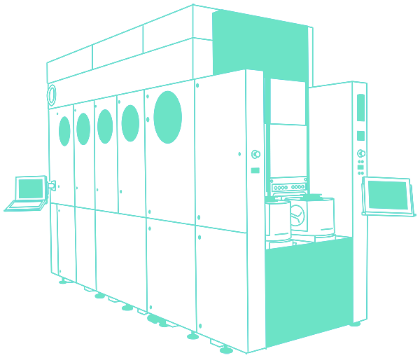
Our market-leading products and services enable our
customers to build smaller, faster, more powerful, and more power-efficient electronic devices—the
kind that are driving the proliferation of technology into our everyday lives.
Scroll down to
see how our company and the industry have changed throughout the years.
Company Milestones
Industry Milestones
The 1980s
1980
1980 - Company founded by David K. Lam in Santa Clara, California
1980 - Wafer size:
150 mm
1980 - Global semiconductor sales topped $14 billion
1980 - DRAM density:
64 Kb
1981
1981 - Introduced first product, the AutoEtch
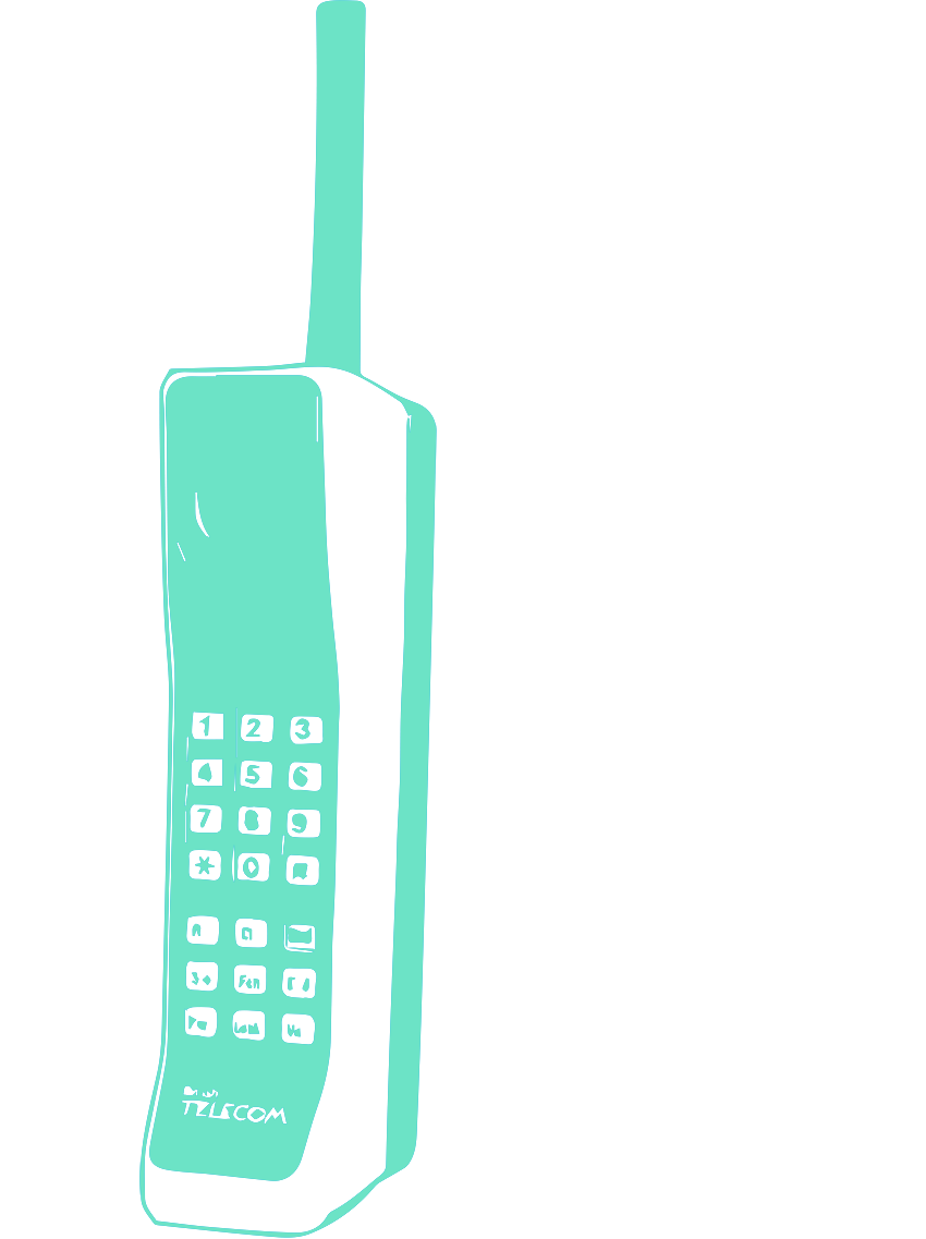
1981 - FCC approved cell phones for commercial development
1982
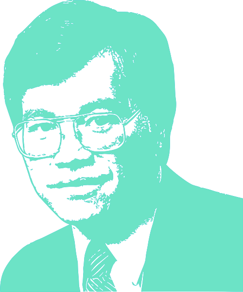
1982 - Roger Emerick appointed as CEO

1982 - Technology node:
1.5 µm
1982 - Number of transistors in a typical microprocessor:
134,000
1984
1984 - Lam became public as LRCX
1985
1985 - Opened first offices in Europe
1985 - Fiscal annual revenue:
~$34 million
1986
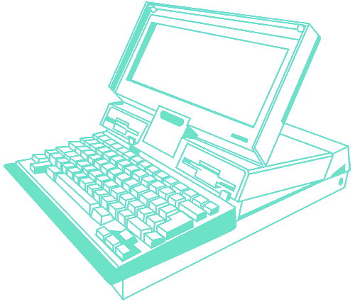
1986 - IBM introduced its first laptop computer, the PC Convertible
1987
1987 - Relocated headquarters to Fremont, California
1987 - Introduced Rainbow® etch system
1987 - Introduced first MSSD system, Concept One® PECVD
1988
1988 - Invented single-wafer spin clean technology
1988 - DRAM density:
4 Mb
1989
1989 - Opened first office in S. Korea
1989 - Technology node:
0.8 µm
1989 - Number of transistors in a typical microprocessor:
1.2 million
The 1990s
1990
1990 - Fiscal annual revenue:
~$140 million
1990 - Introduced SP Series spin clean systems
1990 - Wafer size:
200 mm
1992
1992 - Opened offices in Taiwan and Singapore

1992 - Introduced first Transformer Coupled Plasma™ conductor etch products
1993
1993 - Released Concept Two® ALTUS® CVD tungsten system

1993 - Opened process development center in Japan
1993 - Number of transistors in a typical microprocessor:
3.1 million
1994
1994 - Established presence in China
1994 - DRAM density:
16 Mb
1994 - Global semiconductor sales surpassed $100 billion
1995
1995 - Introduced first Dual Frequency Confined™ dielectric etch product
1995 - Fiscal annual revenue:
~$1.0 billion
1995 - Technology node:
350 nm
1995 - Microsoft introduced Windows 95
1996
1996 - Introduced SPEED® HDP-CVD system
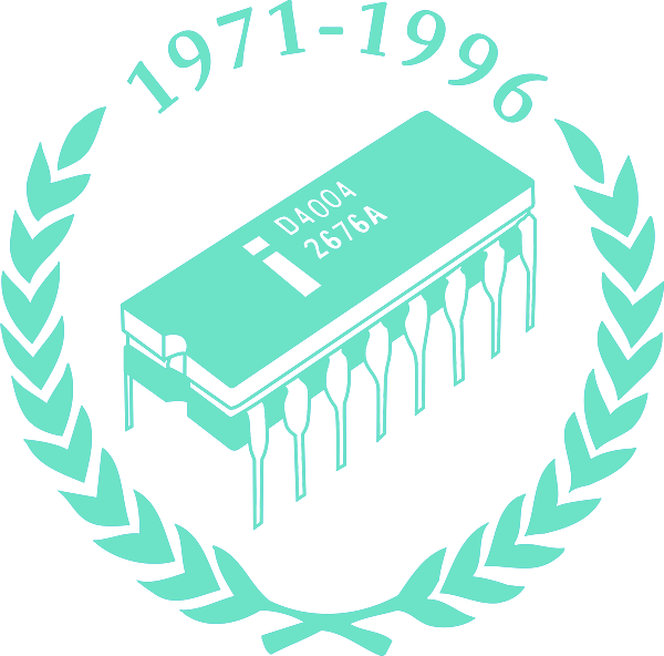
1996 - 25th anniversary of the microprocessor
1997
1997 - Jim Bagley appointed as CEO
1997 - Number of transistors in a typical microprocessor:
7.5 million
1998

1998 - Introduced Lam's Core Values
1998 - Announced SABRE® ECD system
1999
1999 - Technology node:
180 nm
The 2000s
2000
2000 - Announced 2300® etch platform
2000 - Launched VECTOR® PECVD system

2000 - Opened office in India
2000 - Established Lam Research Foundation
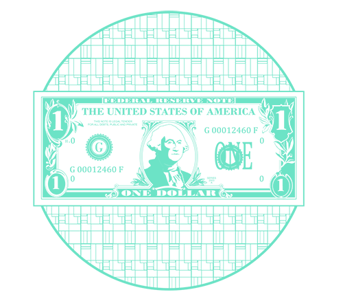
2000 - Fiscal annual revenue:
~$1.2 billion
2000 - Wafer size:
300 mm
2000 - DRAM density:
128 Mb
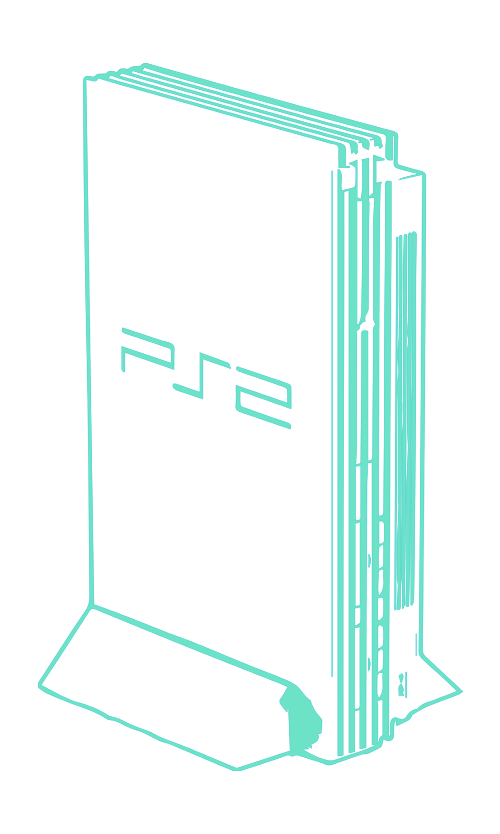
2000 - Sony's Playstation 2 went on sale
2001
2001 - Technology node:
130 nm
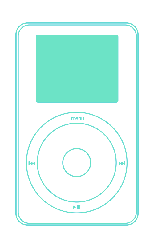
2001 - Apple introduced the iPod music player
2002
2002 - Opened Tualatin, Oregon, campus
2003
2003 - Launched Da Vinci® spin clean product
2004
2004 - Introduced first-generation Kiyo® and Flex® etch products
2004 - Introduced ALTUS® tungsten barrier CVD system
2004 - Technology node:
90 nm
2004 - Global semiconductor sales topped $210 billion
2005
2005 - Launched SOLA® UVTP film treatment system
2005 - Steve Newberry appointed as CEO
2005 - Fiscal annual revenue:
~$1.5 billion
2005 - Number of transistors in a typical microprocessor:
291 million
2005 - DRAM density:
512 Mb
2006
2006 - Acquired Bullen Semiconductor, now Silfex, Inc.
2006 - Technology node:
65 nm
2007
2007 - Shipped first Syndion® system for through-silicon via etch
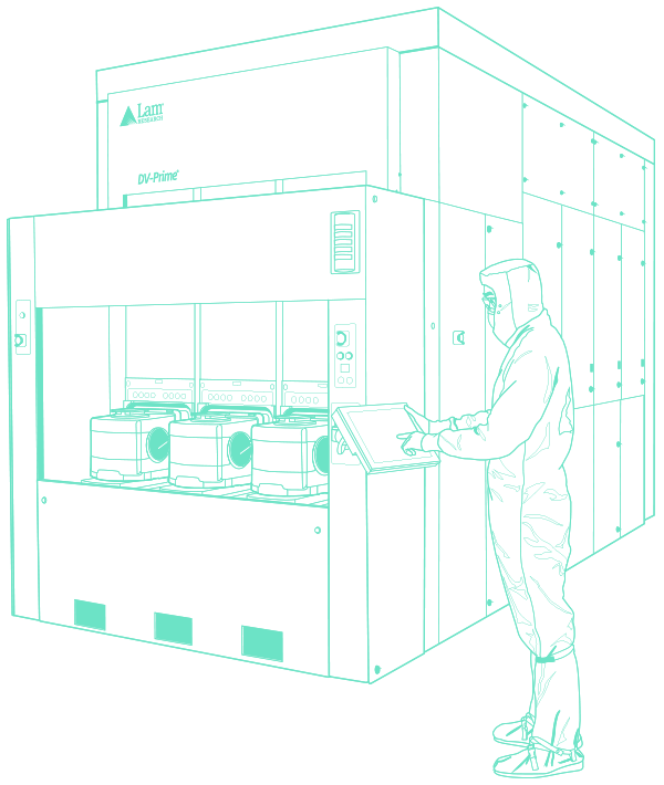
2007 - Introduced DV-Prime® spin clean system
2007 - Launched Coronus® plasma bevel clean system
2007 - Apple unveiled the iPhone
2007 - Number of transistors in a typical microprocessor:
820 million
2008
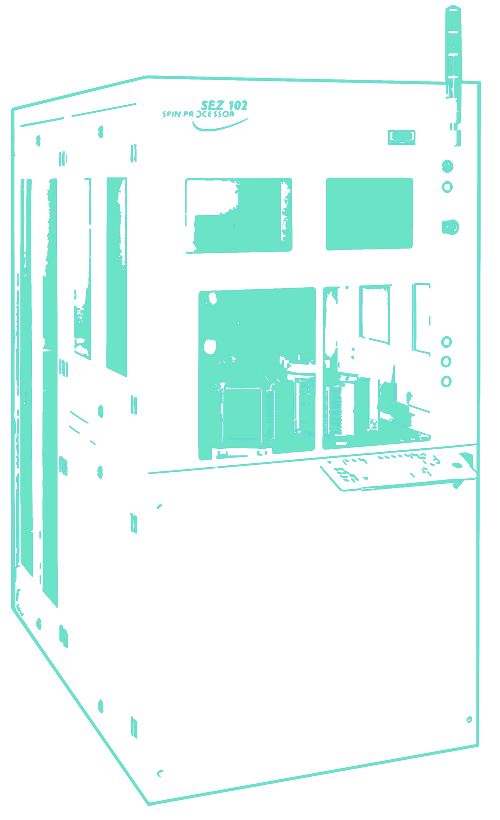
2008 - Acquired SEZ AG, now Lam Research AG
2008 - Introduced GAMMA® GxT® and GAMMA® G400® strip systems
2008 - DRAM density:
1 Gb
The 2010s
2010
2010 - Announced SABRE® 3D ECD system for wafer-level packaging
2010 - Fiscal annual revenue:
~$2.1 billion
2010 - Technology node:
32 nm
2010 - Global semiconductor sales reached ~$300 billion
2011

2011 - Established Corus, now Lam Manufacturing Korea
2012
2012 - Martin Anstice appointed as CEO
2012 - Acquired Novellus Systems
2013
2013 - ~64 billion semiconductors sold in the U.S., or ~200 chips per person
2013 - DRAM density:
4 Gb
2014
2014 - Introduced product suite for 3D NAND: ALTUS® Max ICEFill™ W-CVD, VECTOR® Strata® PECVD, Flex® F Series dielectric etch
2014 - Introduced solutions for multiple patterning: VECTOR® , Kiyo® F Series conductor etch products
2014 - Announced first manufacturing-worthy atomic layer etch: Kiyo® F Series system

2014 - Technology node:
14 nm
2014 - Number of transistors in a typical microprocessor:
4.3 billion
2014 - Wearable tech became mainstream
2015
2015 - Fiscal annual revenue:
~$5.3 billion
2015 - 50th anniversary of Moore's Law
2016
2016 - Opened the Lam Research Dr. Richard A. Gottscho Laboratory in Fremont

2016 - Launched Lam Research Capital
2016 - Technology node:
10 nm
2017
2017 - Acquired
Coventor, Inc.
2017 - 3D NAND:
64 layers
2018
2018 - Tim Archer appointed as CEO
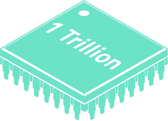
2018 - ~1 trillion semiconductors shipped worldwide
2019

2019 - Achieved new industry benchmark for etch system uptime
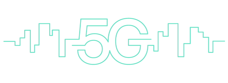
2019 - 5G began deploying worldwide
2020

2020 - Lam's 40th Year Anniversary
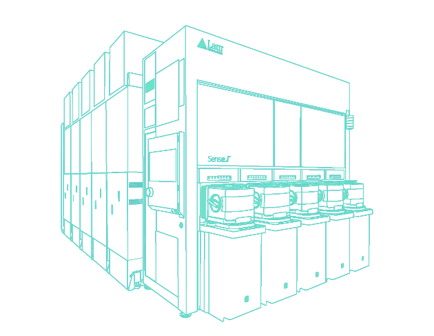
2020 - Announced Sense.i™ plasma etch system
2020 - Developed new dry resist technology with ASML and IMEC
2020 - Remote work and learn trends drove electronics demand
2021

2021 - Set goal to achieve carbon net zero by 2050
2021 - Opened manufacturing facility in Malaysia

2021 - 50th anniversary of the microprocessor
2022
2022 - Opened Korea Technology Center