
스마트폰, 태블릿, 컴퓨터, 게임기 등 전자 기기의 확산은 기술의 미래를 빠르게 변화시키고 있습니다. AI(인공지능)의 발전은 더 효율적이고 강력한 프로세싱 하드웨어에 대한 수요를 이끌고 있습니다. 반도체 제조 기술의 주요 발전은 소형화, 비용 대비 성능 향상, 그리고 연결성 확대에 초점을 맞추고 있습니다.
첨단 패키징 기술과 칩렛 설계는 차세대 전자기기의 고도화된 기술적 요구를 충족하는 데 필수적입니다. 웨이퍼 레벨 패키징(WLP), 3D 실리콘 관통 전극(TSV), 하이브리드 본딩과 같은 기술이 주목받고 있으며, 이를 통해 이기종 통합 및 시스템 인 패키지(SiP) 솔루션이 가능해지고 있습니다. 생성형 AI로 인한 컴퓨팅 성능 수요의 폭발적인 증가는 패키지 크기의 한계를 확장하고 있으며, 이는 고성능 컴퓨팅(HPC)의 미래를 위한 대형 패널 레벨 패키징과 고급 유리 기판의 토대가 되고 있습니다. 이러한 혁신을 통해 여러 칩을 하나의 패키지에 통합함으로써, 새로운 성능 기준과 설계 요구를 충족하는 혁신이 가속화되고 있습니다.
Packaging
램리서치의 솔루션WETS 제품군
포토레지스트 제거, 식각 및 세정 등 전해 도금 공정 전반에 걸쳐 업계를 선도하는 솔루션 제공
DV-Prime & Da Vinci 제품군
Wet Clean
제조 전반에 걸쳐 웨이퍼 세정의 여러 단계를 높은 생산성으로 처리하는 데 필요한 공정 유연성을 갖추고 있습니다.
SP 시리즈 제품군
Wet Clean
성능이 검증된 이 제품군은 뛰어난 신뢰성과 비용 효과로 웨이퍼에서 불필요한 물질을 부드럽게 제거하는 습식 세정/습식 식각 솔루션입니다.
SABRE 제품군
Electrochemical Deposition (ECD)
이 제품군은 업계 최고의 생산성을 자랑하는 ECD 플랫폼에서 구리 다마신을 제조할 때 필요한 고정밀 금속 도금 기능이 있습니다.
SABRE 3D 제품군
Electrochemical Deposition (ECD)
이 고생산성 시스템은 램리서치의 검증된 전기충진(Electrofill) 기술을 사용하여 첨단 패키징 분야에 필요한 양질의 금속막을 만듭니다.
건식 식각 솔루션
TSV, TDV, TGV 와 같은 고종횡비 식각 및 플라즈마 다이싱 등 첨단 패키징 분야에서 기술적으로 복잡한 기술 요구 사항을 극복하는 고생산성 솔루션

FLEX 제품군
Atomic Layer Etch (ALE) Reactive Ion Etch (RIE) 극저온 식각 극저온 식각
램리서치의 유전체 식각 시스템은 용도에 맞춘 기능 덕분에 고급 소자의 까다로운 구조를 다양하게 만들 수 있습니다.

KIYO 제품군
Reactive Ion Etch (RIE)
시장을 선도하는 램리서치의 전도체 식각 제품은 주요 소자 피처(feature)에 요구되는 고성능 정밀도와 제어력이 특징입니다.
Syndion 제품군
Deep Reactive Ion Etch (DRIE) Reactive Ion Etch (RIE)
딥 식각 응용 부문에서 이 제품군은 고종횡비 피처를 형성하는 데 필요한 우수한 웨이퍼 균일도 제어 능력을 제공합니다.
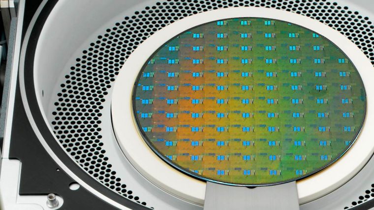
유전체 및 금속 증착
PECVD, ALD, 및 CVD 금속 증착 공정을 위한 차별화된 솔루션 고유전율 절연체, 고접착력 다이 부착층, 저유전율 필름, 열 응력 및 얇은 웨이퍼 스트레스 제어를 위한 다양한 필름 솔루션
Striker 제품군
원자층 증착(ALD)
첨단 ALD 기술을 사용하여 나노 수준의 피처가 있는 고급 소자의 주요 공정을 완벽하게 제어하는 유전막을 제공합니다.

VECTOR 제품군
Plasma-Enhanced Chemical Vapor Deposition (PECVD)
램리서치의 PECVD 제품군은 광범위한 소자 분야에서 높은 생산성으로 고정밀 유전막 증착을 실현합니다.
ALTUS 제품군
Chemical Vapor Deposition (CVD) 원자층 증착(ALD)
CVD 및 ALD 기술을 결합하여 시장을 선도하는 이 시스템은 고급 텅스텐 금속화 응용 분야를 위한 고도의 등각 금속 박막을 증착합니다.
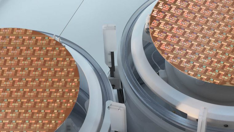
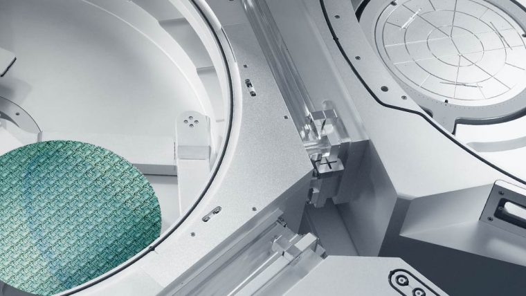
수율 향상 및 공정 제어
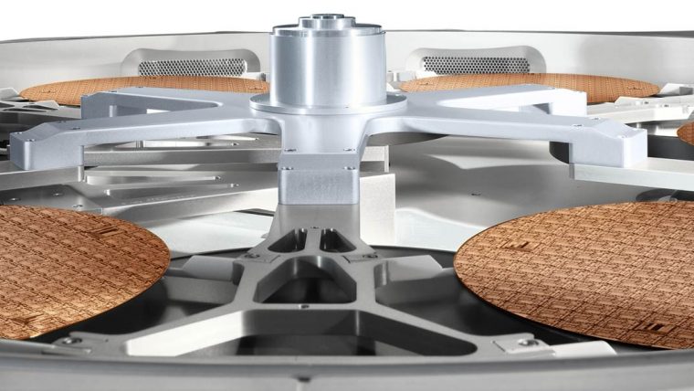
웨이퍼 투 웨이퍼 본딩 수율 향상을 위한 웨이퍼 베벨 관리 및 대량 계측을 통한 고처리량 공정 제어 기능과 같은 첨단 패키징 응용 기술의 과제를 해결하는 혁신적인 솔루션

CORONUS 제품군
Advanced Packaging Plasma Bevel Etch and Deposition
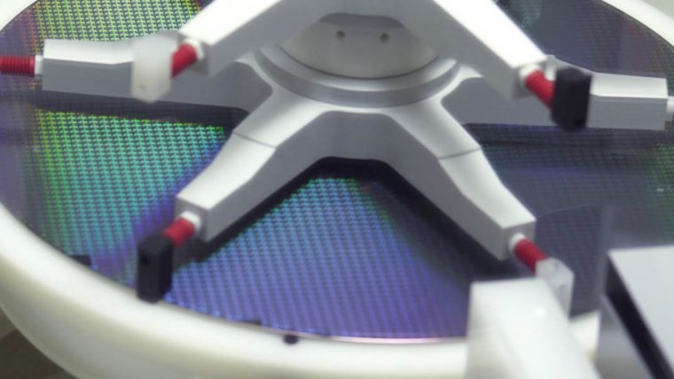
Coronus 시스템은 웨이퍼 베벨 엣지에 중점을 두어 전반적인 수율을 높입니다. 반도체 공정 진행 시 웨이퍼 가장자리를 따라 잔여물과 거칠기가 누적됩니다. 이는 웨이퍼의 다른 영역으로 떨어져 날리면 장치의 고장을 유발하는 결함을 발생시킬 수 있습니다. Coronus 식각 제품은 웨이퍼 베벨에 있는 잔여물을 제거하고 Coronus 증착 제품은 웨이퍼 베벨이 손상되지 않도록 보호합니다.

METRYX 제품군
Mass Metrology
램리서치의 질량 계측 시스템에는 3차원 소자 구조의 첨단 공정 모니터링과 제어에 필요한 밀리그램 미만 단위의 측정 기능이 있습니다.
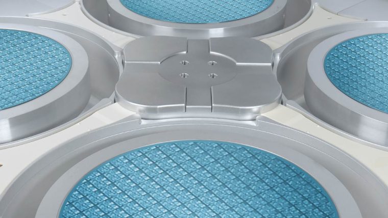
패널 공정 솔루션
웨이퍼 레벨 공정 기술, 성능 및 생산 수율을 패널 레벨 공정으로의 전환 Cu RDL, 마이크로 범프, TGV 및 Cu 적층 전기도금, PR/PI 제거 및 현상 등 습식 패널 공정을 위한 차별화된 솔루션 제공
Phoenix 제품군
Electrochemical Deposition (ECD) PR-Development PR-Strip Wet Clean/Strip/Etch
Phoenix는 510x510mm 기판의 완전 자동화된 대량 패널 처리를 제공합니다.
Kallisto 제품군
Electrochemical Deposition (ECD)
300x300mm에서 1100x1100mm(5.1세대)까지 기판의 습식 화학 처리를 위한 첨단 수직 공정 플랫폼으로 반도체 업계의 요구 사항에 맞게 제작되었습니다.