
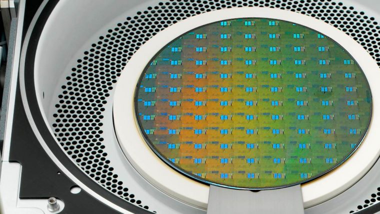
Die Zukunft der Technologie wird durch die zunehmende Verbreitung elektronischer Geräte geprägt, von Smartphones und Tablets bis hin zu Computern und Gaming-Systemen. Das Verlangen nach künstlicher Intelligenz (KI) erhöht den Bedarf an effizienterer und leistungsfähigerer Verarbeitungshardware. Die wichtigsten Fortschritte in der Halbleiterfertigung konzentrieren sich auf die Bereiche Miniaturisierung, Kosten-Nutzen-Verhältnis und Konnektivität.
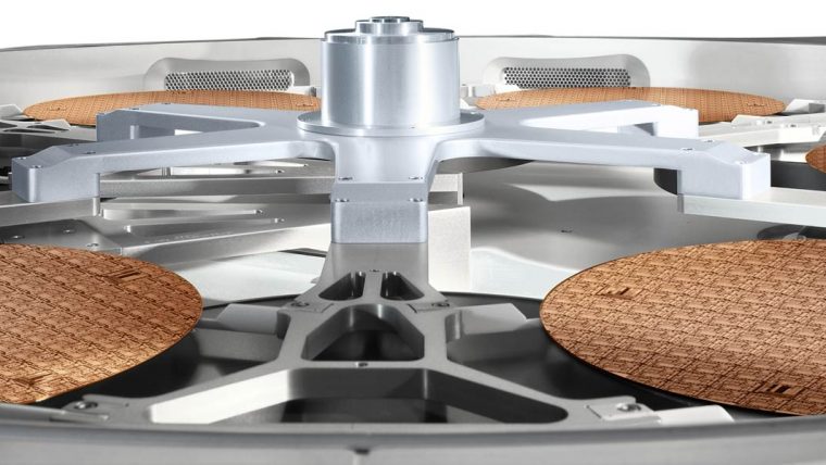
Fortschrittliche Packaging-Technologien und Chiplet-Designs sind unerlässlich, um die Anforderungen von Geräten der nächsten Generation zu erfüllen. Technologien wie Wafer-Level-Packaging (WLP), 3D-Silizium-Durchkontaktierung (TSV) und Hybrid-Bonding gewinnen an Bedeutung und ermöglichen heterogene Integrations- und System-in-Package(SiP)-Lösungen. Die unersättliche Nachfrage nach Rechenleistung, die nicht zuletzt von der generativen KI befeuert wird, verschiebt die Grenzen der Gehäusegrößen und ebnet den Weg für das großformatige Panel-Level-Packaging und fortschrittliche Glassubstrate als Zukunft des High-Performance-Computing (HPC). Diese Innovationen ermöglichen die Integration mehrerer Chips in ein einziges Gehäuse und läuten damit eine neue Ära in puncto Geräteleistung und Design ein.
Packaging
Unsere LösungenWETS-Produktlinie
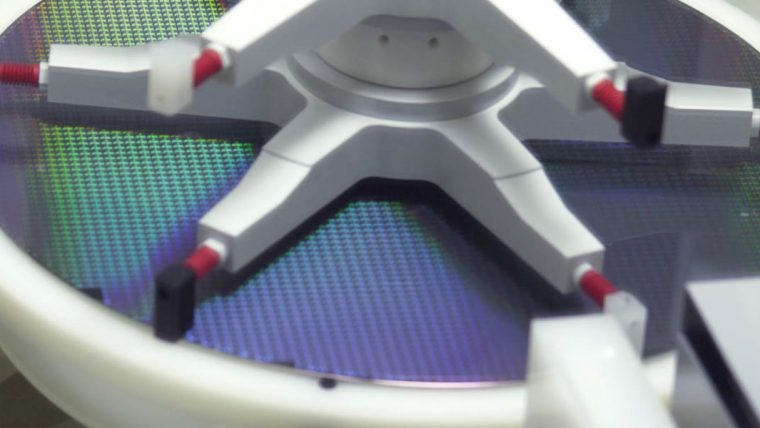
Bereitstellung führender Lösungen in der Galvanisierung und Nassverarbeitung, einschließlich Entfernen von Fotolackrückständen, Ätzen und Reinigen
DV-PRIME UND DA VINCI
Produktfamilie
Wet Clean
Diese Produkte bieten die Prozessflexibilität, die bei hoher Produktivität erforderlich ist, um mehrere Waferreinigungsschritte in der gesamten Fertigung abzudecken.
SP-SERIE Produktfamilie
Wet Clean
Diese bewährte Produktfamilie bietet zuverlässige, kostengünstige Nassreinigungs- / Nassätzlösungen, mit denen unerwünschte Materialien vorsichtig vom Wafer entfernt werden.
SABRE Produktfamilie
Elektrochemische Abscheidung (ECD)
Diese Produktfamilie bietet auf der produktivitätsführenden ECD-Plattform der Branche Präzisionsmetallisierung für die Kupfer-Damascene-Herstellung.
SABRE 3D Produktfamilie
Elektrochemische Abscheidung (ECD)
Dank unserer bewährten Electrofill-Technologie liefern diese hochproduktiven Systeme hochwertige Metallfolien für moderne Verpackungsanwendungen.
Trockenätzlösungen
Hochproduktive Lösungen zur Bewältigung technisch anspruchsvoller Anforderungen beim Advanced Packaging, z. B. Ätzen bei hohem Aspektverhältnis (TSV, TDV & TGV) und Plasma-Dicing

FLEX PRODUKTFAMILIE
Atomic Layer Etch (ALE) Kryogenes Ätzen Reaktive Ionenätzung (RIE)
Die dielektrischen Ätzsysteme von Lam bieten anwendungsorientierte Funktionen zum Erstellen einer Vielzahl anspruchsvoller Strukturen in modernen Geräten.
GAMMA Produktfamilie
Dry Strip
Diese Produkte bieten die Prozessflexibilität, die erforderlich ist, um ein breites Spektrum kritischer Photoresiststreifenanwendungen abzudecken.

Kiyo PRODUKTFAMILIE
Reaktive Ionenätzung (RIE)
Diese marktführenden Leiterätzungsprodukte bieten höchste Präzision und Kontrolle bei hoher Produktivität, die für kritische Gerätefunktionen erforderlich sind.
Syndion-Produktfamilie
Reaktive Ionenätzung (RIE) Tiefe reaktive Ionenätzung (DRIE)
Für Tiefenätzanwendungen bietet diese Produktfamilie die außergewöhnliche Wafer-zu-Wafer-Gleichmäßigkeit, die für kritische Features mit hohem Querschnittsverhältnis unabdingbar ist.
Dielektrische und Metallabscheidung
Differenzierte Lösungen für PECVD-, ALD- und CVD-Metalle. Ermöglicht verschiedene Folienanforderungen für Advanced Packaging, einschließlich dielektrischer Schichten mit hoher Haftkraft, hochwertiger Inter-Die-Gapfill-Folien und anpassbarer Folienspannung für Wafer-Stress- und Formmanagement
STRIKER Produktfamilie
Atomlagenabscheidung (ALD)
Mit der fortschrittlichen ALD-Technologie liefern diese Produkte dielektrische Filme mit hervorragender Kontrolle für kritische Prozesse in fortschrittlichen Geräten mit Nanomaßstab.

Vector Produktfamilie
Plasmaunterstützte chemische Gasphasenabscheidung (PECVD)
Unsere PECVD-Produktfamilie ermöglicht eine präzise dielektrische Filmabscheidung bei hoher Produktivität für eine Vielzahl von Anwendungen.
ALTUS Produktfamilie
Atomlagenabscheidung (ALD) Chemische Gasphasenabscheidung (CVD)
Durch die Kombination von CVD- und ALD-Technologien tragen diese marktführenden Systeme in hohem Grad konforme Metallschichten für moderne Wolfram-Metallbeschichtungsanwendungen auf.
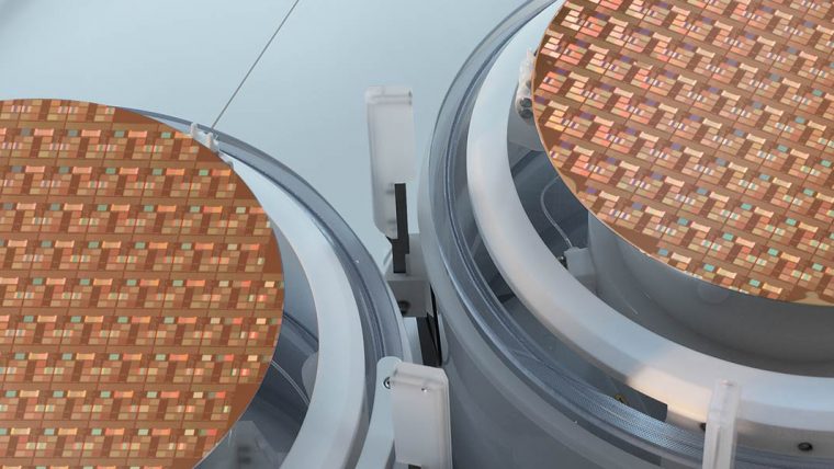
Ertragsverbesserung und Prozesskontrolle
Innovative Lösungen zur Bewältigung der Herausforderungen neuer Advanced-Packaging-Anwendungen, z. B. Waferrand-Management für die Verbesserung der Waferbonding-Ausbeute und Prozesskontrollfähigkeit mit hohem Durchsatz und Massenmetrologie

CORONUS Produktfamilie
Plasma Bevel Etch and Deposition
Der Schwerpunkt der Coronus-Systeme liegt auf der Schrägkante und damit auf der Verbesserung der Ausbeute insgesamt. Die Halbleiterverarbeitung kann das Anhäufen von Rückständen sowie die Entstehung rauer Oberflächen entlang dem Waferrand bewirken, von dem aus die Rückstände abblättern, in andere Bereiche abdriften und Defekte verursachen können, die einen Geräteausfall zur Folge haben. Coronus-Ätzprodukte entfernen diese Rückstände auf den Rändern und Coronus Deposition schützt den Waferrand vor Beschädigungen.

METRYX PRODUKTFAMILIE
Mass Metrology
Unsere Massemesssysteme bieten Messmöglichkeiten im Milligrammbereich für erweiterte Prozessüberwachung und Steuerung dreidimensionaler Gerätestrukturen.
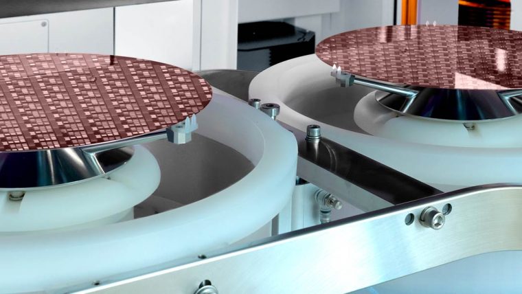
Lösungen für die Plattenverarbeitung
Übertragung von Prozesstechnologie, Leistung und Produktionsausbeute auf Wafer-Ebene auf die Panel-Level-Verarbeitung. Lieferung differenzierter Lösungen für die Nassplattenverarbeitung, z. B. Cu RDL, Micro-Bump, TGV und Cu-Build-up-Galvanisierung, Entfernen von Fotolackrückständen, Ätzen, Aufrauen und Reinigen.
Kallisto-Produktfamilie
Elektrochemische Abscheidung (ECD)
Eine fortschrittliche vertikale Prozessplattform für die nasschemische Behandlung von Substraten von 300 x 300 mm bis hin zu Gen 5.1 (1100 x 1300 mm), die auf die Bedürfnisse der Halbleiterindustrie zugeschnitten ist.
Phoenix-Produktfamilie
Elektrochemische Abscheidung (ECD) Fotolack-Entwicklung Fotolack-Strippen Nassreinigung/Strippen/Ätzen
Phoenix bietet eine vollautomatische, hochvolumige Plattenverarbeitung für 510×515 mm große Substrate an.