從智慧型手機和平板電腦到電腦和遊戲系統,電子設備的日益普及正在塑造技術的未來。 人工智慧(AI)的發展推動了對更有效率、更強大的處理硬體的需求。 半導體製造的關鍵進步集中在小型化、性價比和連接性上。
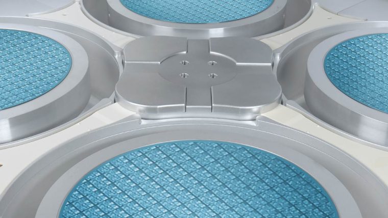
先進的封裝技術和小晶片設計對於滿足下一代元件的需求至關重要。 晶圓級封裝(WLP)、3D 矽穿孔(TSV)互連和混合接合等技術正在獲得關注,從而實現異質整合系統級封裝(SiP)解決方案。 由於生成式人工智慧所驅動對運算能力的無止盡需求,正推動封裝尺寸的極限,為大尺寸面板級封裝和先進玻璃基板鋪路,這些技術被視為高效能運算(HPC)的未來方向。 這些創新技術使多顆晶片能整合於單一封裝中,預示著元件效能和設計進入全新時代。
封裝
我們的解決方案WETS產品線
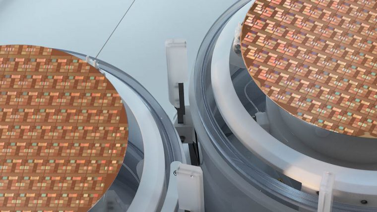
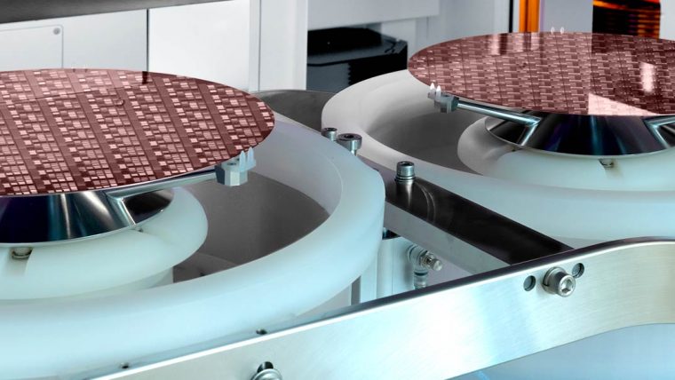
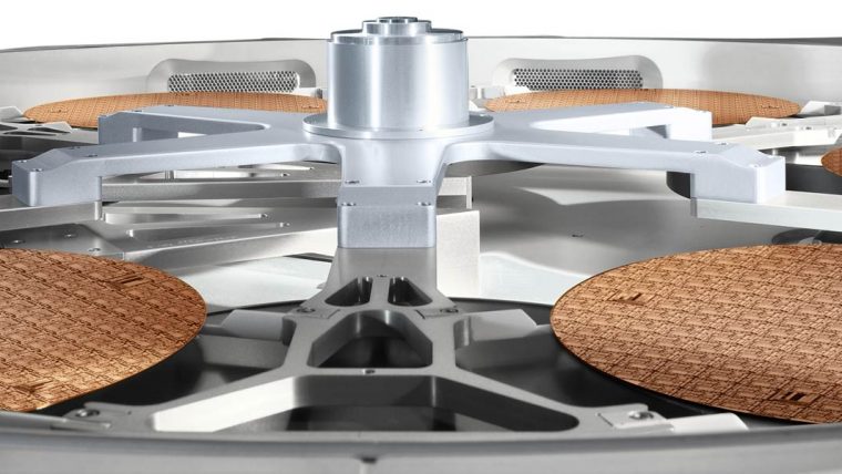
在電鍍和濕式製程上提供領先的解決方案,包括光組移除、蝕刻和清潔
乾式蝕刻解決方案
高生產力解決方案,以克服先進封裝中的技術挑戰要求,如高深寬比刻蝕(TSV、TDV和TGV)和電漿切割


介電層和金屬沉積
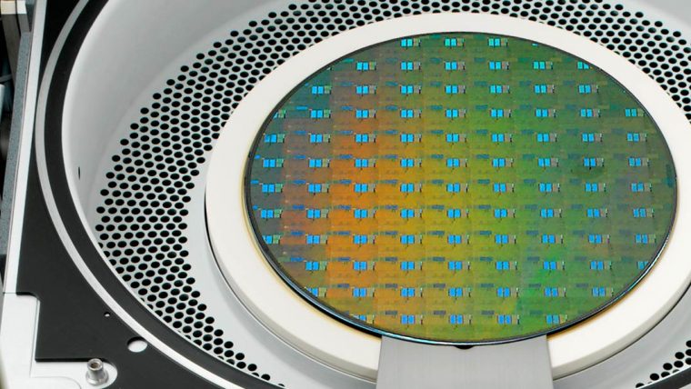
PECVD、ALD 和 CVD 金屬的差異化解決方案。 支援先進封裝的各種薄膜需求,包括高接合強度的介電層、高品質晶粒間隙填充薄膜以及可調整的薄膜應力,以利晶圓應力與形狀管理

良率提升和製程控制
創新解決方案可克服先進封裝應用中的挑戰,例如透過晶圓邊緣管理來提升晶圓對晶圓鍵合良率,以及結合大量量測技術以實現高產能製程控制能力


面板製程解決方案
將晶圓級製程技術、效能與生產良率轉移至面板級製程。 提供差異化的濕式面板製程解決方案,包括銅重分佈線層(Cu RDL)、微凸塊(micro-bump)、玻璃通孔(TGV)與銅堆疊電鍍(Cu build-up electroplating)、光阻/聚醯亞胺(PR/PI)去除/顯影、蝕刻、粗化與清洗等製程。