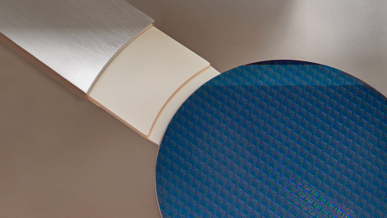
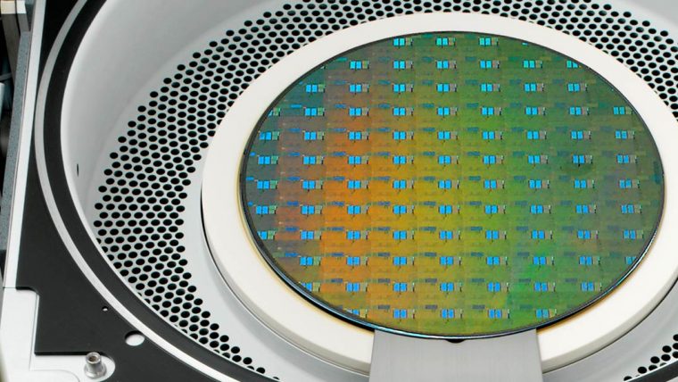
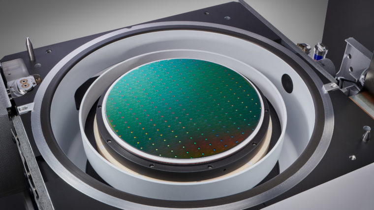
製造具原子級精密度的特徵結構
透過選擇性地去除在沉積期間添加的介電層(絕緣)和金屬(導電)材料,蝕刻製程可用來製作晶片的特徵結構。這些製程涉及製造越來越小、複雜、高且窄的特徵結構,並使用多種類型的材料。主要的技術,反應離子蝕刻 (RIE),是用離子(帶電微粒) 轟擊晶片表面來去除材料。針對最微小的特徵結構,原子層蝕刻 (ALE) 可一次去除一些原子層的材料。而導體蝕刻製程可精確形成電晶體這類的關鍵電子元件,介電層蝕刻則可形成保護導電部分的絕緣結構。蝕刻製程還能創建高的柱狀特徵,例如,用在矽穿孔(TSV)中來連接晶片、以及用在微機電系統(MEMS)中。
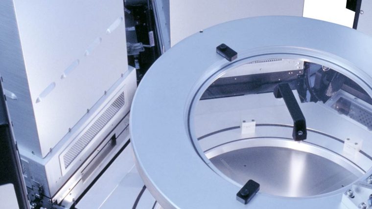
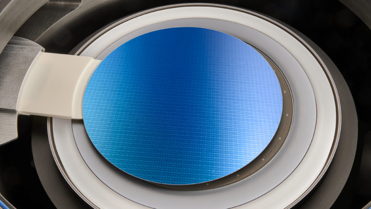
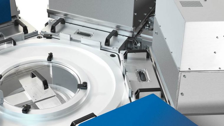
Lam Research的電漿蝕刻系統可提供形成精確結構所需的高效能、高生產力功能 ─ 無論是高且窄、短且寬、還是僅有幾奈米大小的結構均適用。
電漿蝕刻
產品


Related Blog Posts
-

Etch Essentials: The Building Blocks of AI Era Microchips
Jun 12, 2024The artificial intelligence era depends on the storage infrastructure needed to run advanced technology, such as generative AI. The performance requirements for these AI innovations are pushing NAND devices to quickly scale to 400 vertically stacked layers and beyond. For readers who are new to semiconductors, that’s a big deal. Imagine a skyscraper with an unfathomable 400 floors, where each floor represents a layer of memory in a NAND device. Now, imagine adding 600 more floors to that building...only in semiconductors, this super tall structure is still invisible to the naked eye. Today, these devices range in height from a few micrometers (µm) to tens of micrometers.
-
How Etch Is Evolving to Meet the Demands of the AI Era
Nov 8, 2023The rise of artificial intelligence (AI) has placed significant demands on semiconductor performance, particularly in the realm of etching technology. AI requires massive amounts of data for training, necessitating high levels of parallel processing, non-volatile memory, and fast data transfer rates. To achieve these capabilities advanced devices are designed in three dimensions, leading to the need for novel etching techniques. Perpendicular etching, which involves removing materials in multiple directions, is essential for crafting gate-all-around (GAA) transistor architectures and precise modification of atomic layers. Aspect-ratio-dependent etching is crucial for the transition from 2D to 3D NAND architecture, enabling the efficient storage capacity increase by etching through numerous layers.