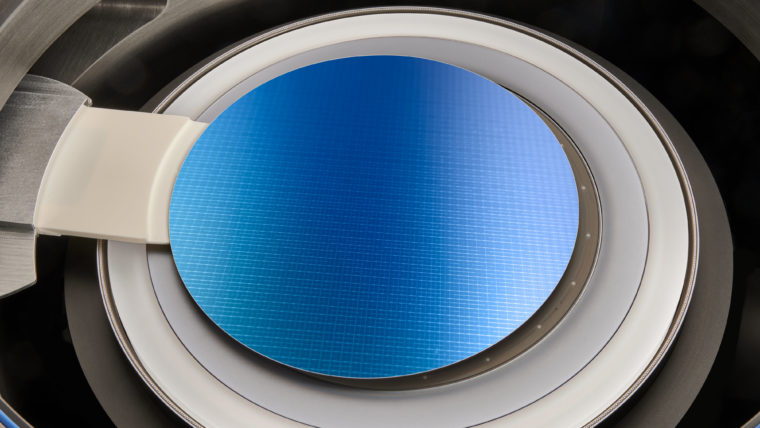
Creating features with atomic precision
Etch processes help create chip features by selectively removing films and materials that have been deposited on the wafer. These processes involve fabricating increasingly small and complex features with complicated combinations of materials that need to be removed. The primary technology, reactive ion etch (RIE), activates the wafer surface with ions (charged particles) to remove material. Advanced etch techniques, such as atomic layer etching (ALE) are capable of removing a few atomic layers of material at a time. While conductor etch processes precisely shape electrically active components like transistors, dielectric etch forms the insulating structures that protect conducting parts. Etch processes also create the tall, high-aspect ratio features, such as through-silicon vias (TSVs), that allow packaging of chips together and for micro-electromechanical systems (MEMS).
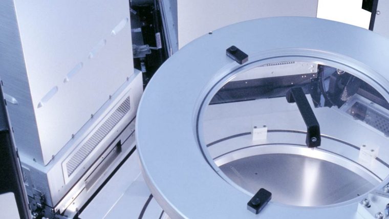
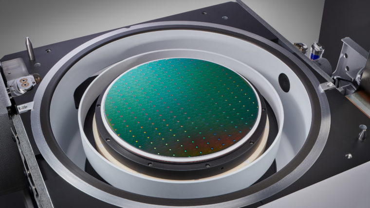
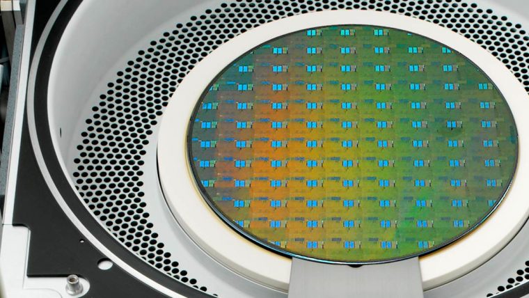
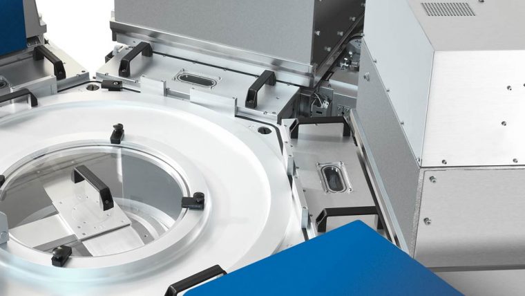
Our plasma etch systems deliver the high-performance, high-productivity capabilities needed to form exacting structures – whether tall and narrow, short and wide, or measured in only a few angstroms.
Etch
Our ProductsAkara®
Conductor Etch
Designed for high-volume production with maximum process yield, Akara® increases wafer output and eliminates wasted time, with millisecond response times to any change. The industry’s most advanced etch uniformity controls provide angstrom-level critical dimension uniformity and wafer to wafer repeatability.

Coronus Product Family
Plasma Bevel Etch and Deposition
Coronus systems focus on the bevel edge to enhance overall yield. Semiconductor processing can cause residues and roughness to accumulate along the wafer edge where they may flake off, drift to other areas, and create defects that cause a device to fail. Coronus etch products remove bevel residues and Coronus deposition protect the wafer bevel from damage.

Flex Product Family
Atomic Layer Etch (ALE) Cryogenic Etching Reactive Ion Etch (RIE)
Our dielectric etch systems offer application-focused capabilities for creating a wide range of challenging structures in advanced devices.

Kiyo Product Family
Reactive Ion Etch (RIE)
These market-leading conductor etch products deliver the high-performance precision and control at high productivity needed for critical device features.
Reliant Etch Products
Deep Reactive Ion Etch (DRIE) Reactive Ion Etch (RIE) Reliant Systems
Our Reliant etch products enable roadmaps for Specialty Technologies and extend the productive life of fabs.
Selective Etch Product Family
Selective Etch
Breakthrough portfolio delivers isotropic material removal with angstrom-scale precision and ultra-high selectivity capabilities for 3D architectures and advanced logic and foundry applications.
Sense.i Product Family
Reactive Ion Etch (RIE)
Our latest etch platform offers unparalleled system intelligence in a compact, high-density architecture to deliver process performance at the highest productivity.
Syndion Product Family
Deep Reactive Ion Etch (DRIE) Reactive Ion Etch (RIE)
For deep etch applications, this product family provides the exceptional across-wafer uniformity control needed for critical high aspect ratio features.
Vantex Product Family
Cryogenic Etching Reactive Ion Etch (RIE)
Designed for the Sense.i platform, Vantex redefines high aspect ratio etching with innovations in technology and Equipment Intelligence.
Versys Metal Product Family
Reactive Ion Etch (RIE)
These metal etch products provide excellent process control at high-productivity for electrical connection and metal hardmask applications.
Related blog posts
-

Etch Essentials: The Building Blocks of AI Era Microchips
Jun 12, 2024The artificial intelligence era depends on the storage infrastructure needed to run advanced technology, such as generative AI. The performance requirements for these AI innovations are pushing NAND devices to quickly scale to 400 vertically stacked layers and beyond. For readers who are new to semiconductors, that’s a big deal. Imagine a skyscraper with an unfathomable 400 floors, where each floor represents a layer of memory in a NAND device. Now, imagine adding 600 more floors to that building...only in semiconductors, this super tall structure is still invisible to the naked eye. Today, these devices range in height from a few micrometers (µm) to tens of micrometers.
-
How Etch Is Evolving to Meet the Demands of the AI Era
Nov 8, 2023The rise of artificial intelligence (AI) has placed significant demands on semiconductor performance, particularly in the realm of etching technology. AI requires massive amounts of data for training, necessitating high levels of parallel processing, non-volatile memory, and fast data transfer rates. To achieve these capabilities advanced devices are designed in three dimensions, leading to the need for novel etching techniques. Perpendicular etching, which involves removing materials in multiple directions, is essential for crafting gate-all-around (GAA) transistor architectures and precise modification of atomic layers. Aspect-ratio-dependent etching is crucial for the transition from 2D to 3D NAND architecture, enabling the efficient storage capacity increase by etching through numerous layers.