
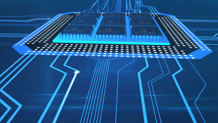
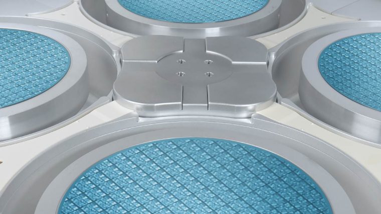
Transistors – the “brains” of a chip – are tiny switches that control the flow of electricity, and there can literally be billions of these on a single integrated circuit. Demand for smaller, more powerful electronics is driving the development of new transistor architectures like 3D FinFET designs and the use of specialty materials such as high-k/metal gates. These in turn allow continued shrinking of device feature sizes. With dimensions for the latest transistors now at the atomic level, they are extremely challenging to manufacture. To ensure the high performance expected of these advanced devices, manufacturing capabilities that deliver exceptional precision and control in forming the tiny features are needed.
Transistor
Our Solutions
ALTUS Product Family
Atomic Layer Deposition (ALD) Chemical Vapor Deposition (CVD)
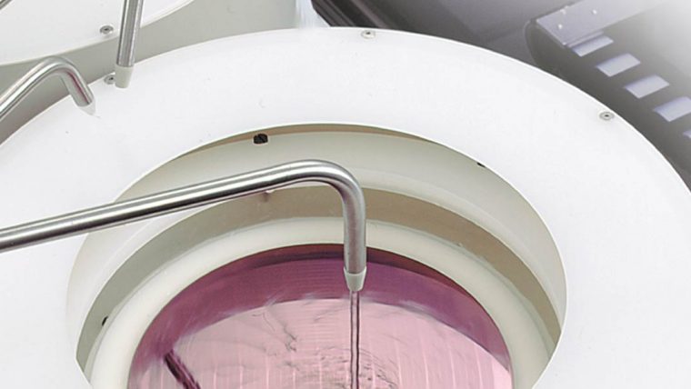
Combining CVD and ALD technologies, these market-leading systems deposit highly conformal metal films for advanced tungsten metallization applications.

Coronus Product Family
Plasma Bevel Etch and Deposition
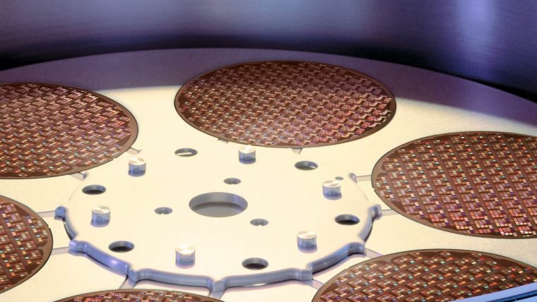
Coronus systems focus on the bevel edge to enhance overall yield. Semiconductor processing can cause residues and roughness to accumulate along the wafer edge where they may flake off, drift to other areas, and create defects that cause a device to fail. Coronus etch products remove bevel residues and Coronus deposition protect the wafer bevel from damage.
DV-Prime & Da Vinci Product Families
Wet Clean
These products provide the process flexibility needed with high productivity to address multiple wafer cleaning steps throughout manufacturing.
EOS Product Family
Wet Clean
Our advanced wet clean products deliver exceptionally low on-wafer defectivity at high throughput for progressively demanding applications.

Fabtex™ Yield Optimizer
Semiconductor Yield Optimization Platform
Fabtex™ Yield Optimizer is a cutting-edge software platform designed to help semiconductor foundries accelerate yield ramp and improve high-volume manufacturing performance.

Flex Product Family
Atomic Layer Etch (ALE) Cryogenic Etching Reactive Ion Etch (RIE)
Our dielectric etch systems offer application-focused capabilities for creating a wide range of challenging structures in advanced devices.
GAMMA Product Family
Dry Strip
These products provide the process flexibility needed to address a wide range of critical photoresist strip applications.

Kiyo Product Family
Reactive Ion Etch (RIE)
These market-leading conductor etch products deliver the high-performance precision and control at high productivity needed for critical device features.

Metior Product Family
Mass Metrology
Our mass metrology systems deliver sub-milligram measurement capability for advanced process monitoring and control of three-dimensional device structures.

OverViz
Plasma Modeling
OverViz™ is an industrial simulation software platform for high-fidelity modeling of plasma discharges.
Reliant Clean Products
Reliant Systems Wet Clean/Strip
Our Reliant clean products enable roadmaps for Specialty Technologies and extend the productive life of fabs.
Reliant Deposition Products
Chemical Vapor Deposition (CVD) High-Density Plasma Chemical Vapor Deposition (HDP-CVD) Plasma-Enhanced Chemical Vapor Deposition (PECVD) Pulsed Laser Deposition (PLD) Reliant Systems
Our Reliant deposition products enable roadmaps for Specialty Technologies and extend the productive life of fabs.
Reliant Etch Products
Deep Reactive Ion Etch (DRIE) Reactive Ion Etch (RIE) Reliant Systems
Our Reliant etch products enable roadmaps for Specialty Technologies and extend the productive life of fabs.
Selective Etch Product Family
Selective Etch
Breakthrough portfolio delivers isotropic material removal with angstrom-scale precision and ultra-high selectivity capabilities for 3D architectures and advanced logic and foundry applications.
SEMulator3D
Semiconductor Process Modeling
SEMulator3D® is a semiconductor process modeling platform that offers wide ranging technology development capabilities.
Sense.i Product Family
Reactive Ion Etch (RIE)
Our latest etch platform offers unparalleled system intelligence in a compact, high-density architecture to deliver process performance at the highest productivity.
SOLA Product Family
Ultraviolet Thermal Processing (UVTP)
This product family offers specialized post-deposition film treatments to improve physical characteristics for advanced film applications.
SPEED Product Family
High-Density Plasma Chemical Vapor Deposition (HDP-CVD)
These dielectric deposition products provide complete gapfill of high aspect ratio spaces with industry-leading throughput and reliability.
Striker Product Family
Atomic Layer Deposition (ALD)
Using advanced ALD technology, these products deliver dielectric films with exceptional control for critical processes in advanced devices with nanoscale features.

VECTOR Product Family
Plasma-Enhanced Chemical Vapor Deposition (PECVD)
Our PECVD product family provides precise dielectric film deposition at high productivity for a wide range of device applications.
Related Blog Posts
-
Understanding CFETs, a Next Generation Transistor Architecture
Mar 21, 2024Computing power has experienced exponential growth over the last 70 years. This has largely been achieved through transistor scaling. Due to a continuous reduction in the size of transistors, engineers have been able to pack more and more of them onto a single chip[1]. This has led to faster, more powerful, and more energy-efficient devices. Improvements in fabrication processes and materials, along with better circuit design techniques, have enabled this scaling. As transistors have become smaller and more densely packed, we have started to reach limitations caused by the laws of physics.
-
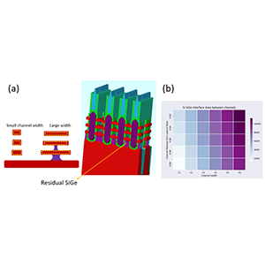
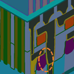
Improving Gate All Around (GAA) Transistor Performance using Virtual Process Window Exploration
Jun 14, 2023As transistor sizes shrink, short channel effects make it more difficult for transistor gates to turn a transistor ON and OFF [1]. One method to overcome this problem is to move away from planar transistor architectures toward 3D devices. Gate-all-around (GAA) architectures are an example of this type of 3D device [2]. In a GAA transistor, the gate oxide surrounds the channel in all directions. A key process during the fabrication of GAA transistors involves the channel release step.