
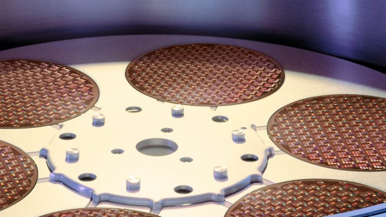
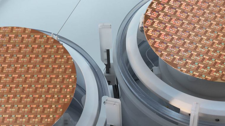
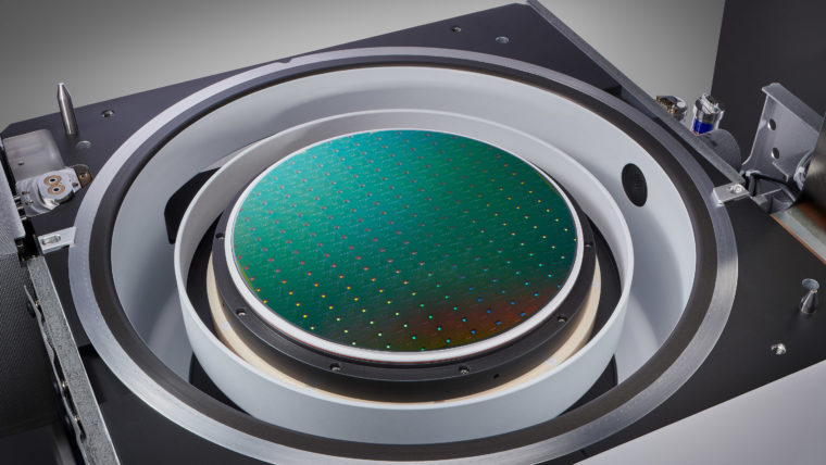
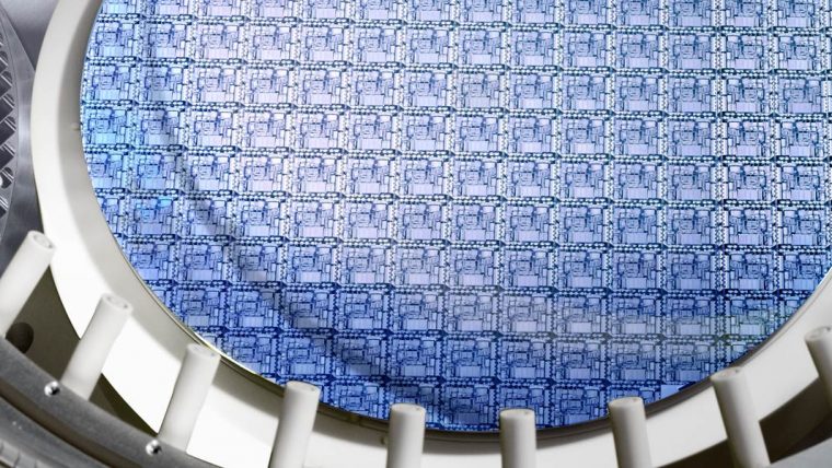
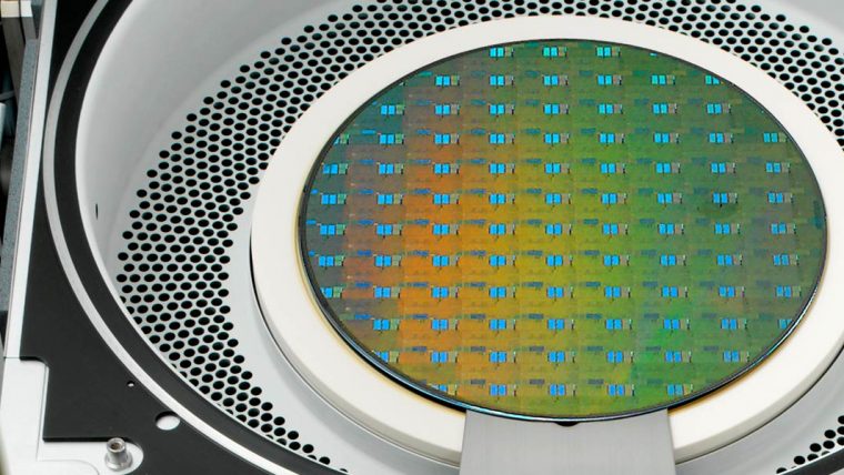
The interconnect makes up the intricate wiring that connects the billions of individual components (transistors, capacitors, etc.) on a chip. As smaller and smaller devices are packed closer together, more interconnect levels are needed, and connecting everything becomes increasingly challenging. In fact, as the shrinking of feature dimensions has continued, interconnects are now becoming the speed bottleneck in today’s most advanced chips. As a result, techniques that minimize resistance of the metal connections and novel dielectric materials that boost insulating capacity are needed. To produce the latest high-performance electronic devices, advanced interconnect structures involve narrow geometries and complex film layers, which require increasingly flexible and precise process capabilities.
Interconnect
Our Solutions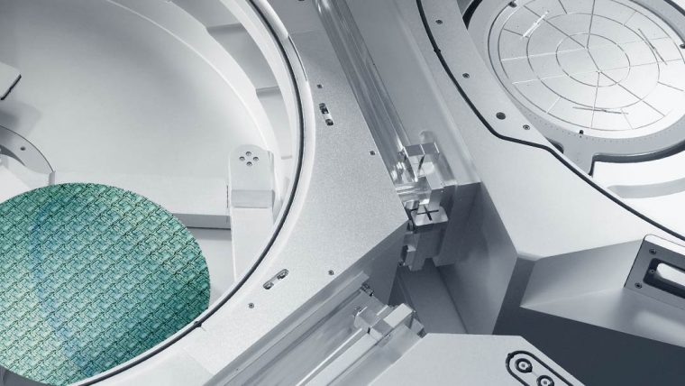
ALTUS Product Family
Atomic Layer Deposition (ALD) Chemical Vapor Deposition (CVD)
Combining CVD and ALD technologies, these market-leading systems deposit highly conformal metal films for advanced tungsten metallization applications.

Coronus Product Family
Plasma Bevel Etch and Deposition
Coronus systems focus on the bevel edge to enhance overall yield. Semiconductor processing can cause residues and roughness to accumulate along the wafer edge where they may flake off, drift to other areas, and create defects that cause a device to fail. Coronus etch products remove bevel residues and Coronus deposition protect the wafer bevel from damage.
DV-Prime & Da Vinci Product Families
Wet Clean
These products provide the process flexibility needed with high productivity to address multiple wafer cleaning steps throughout manufacturing.
EOS Product Family
Wet Clean
Our advanced wet clean products deliver exceptionally low on-wafer defectivity at high throughput for progressively demanding applications.

Fabtex™ Yield Optimizer
Semiconductor Yield Optimization Platform
Fabtex™ Yield Optimizer is a cutting-edge software platform designed to help semiconductor foundries accelerate yield ramp and improve high-volume manufacturing performance.

Flex Product Family
Atomic Layer Etch (ALE) Cryogenic Etching Reactive Ion Etch (RIE)
Our dielectric etch systems offer application-focused capabilities for creating a wide range of challenging structures in advanced devices.
GAMMA Product Family
Dry Strip
These products provide the process flexibility needed to address a wide range of critical photoresist strip applications.

Kiyo Product Family
Reactive Ion Etch (RIE)
These market-leading conductor etch products deliver the high-performance precision and control at high productivity needed for critical device features.

Metior Product Family
Mass Metrology
Our mass metrology systems deliver sub-milligram measurement capability for advanced process monitoring and control of three-dimensional device structures.

OverViz
Plasma Modeling
OverViz™ is an industrial simulation software platform for high-fidelity modeling of plasma discharges.
Reliant Clean Products
Reliant Systems Wet Clean/Strip
Our Reliant clean products enable roadmaps for Specialty Technologies and extend the productive life of fabs.
Reliant Deposition Products
Chemical Vapor Deposition (CVD) High-Density Plasma Chemical Vapor Deposition (HDP-CVD) Plasma-Enhanced Chemical Vapor Deposition (PECVD) Pulsed Laser Deposition (PLD) Reliant Systems
Our Reliant deposition products enable roadmaps for Specialty Technologies and extend the productive life of fabs.
Reliant Etch Products
Deep Reactive Ion Etch (DRIE) Reactive Ion Etch (RIE) Reliant Systems
Our Reliant etch products enable roadmaps for Specialty Technologies and extend the productive life of fabs.
SABRE Product Family
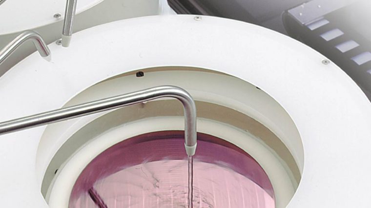
Electrochemical Deposition (ECD)
This product family offers precision metal plating for copper damascene manufacturing on the industry’s productivity-leading ECD platform.
Selective Etch Product Family
Selective Etch
Breakthrough portfolio delivers isotropic material removal with angstrom-scale precision and ultra-high selectivity capabilities for 3D architectures and advanced logic and foundry applications.
SEMulator3D
Semiconductor Process Modeling
SEMulator3D® is a semiconductor process modeling platform that offers wide ranging technology development capabilities.
Sense.i Product Family
Reactive Ion Etch (RIE)
Our latest etch platform offers unparalleled system intelligence in a compact, high-density architecture to deliver process performance at the highest productivity.
SOLA Product Family
Ultraviolet Thermal Processing (UVTP)
This product family offers specialized post-deposition film treatments to improve physical characteristics for advanced film applications.
SPEED Product Family
High-Density Plasma Chemical Vapor Deposition (HDP-CVD)
These dielectric deposition products provide complete gapfill of high aspect ratio spaces with industry-leading throughput and reliability.
Syndion Product Family
Deep Reactive Ion Etch (DRIE) Reactive Ion Etch (RIE)
For deep etch applications, this product family provides the exceptional across-wafer uniformity control needed for critical high aspect ratio features.

VECTOR Product Family
Plasma-Enhanced Chemical Vapor Deposition (PECVD)
Our PECVD product family provides precise dielectric film deposition at high productivity for a wide range of device applications.
Versys Metal Product Family
Reactive Ion Etch (RIE)
These metal etch products provide excellent process control at high-productivity for electrical connection and metal hardmask applications.
Related Blog Posts
-

Will Moly Replace Tungsten in Semiconductors?
Feb 1, 2024To keep pace with Moore's Law and enable greater interconnect scaling, the semiconductor ecosystem is continually experimenting with variations of materials. Tungsten has been the interconnect metal of choice for nearly a quarter century in NAND, DRAM, and logic/foundry middle-of-line applications. But scaling requirements are now pushing the boundaries of what is possible with tungsten. A variety of metals are being considered, but one — molybdenum — is an especially promising candidate. At the atomic dimensions required for advanced chipmaking, moly is emerging as the most suitable material to replace tungsten, creating a major inflection in the industry.
-
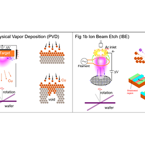
A Deposition and Etch Technique to Lower Resistance of Semiconductor Metal Lines
Mar 22, 2023Cu’s resistivity depends on its crystal structure, void volume, grain boundaries and material interface mismatch, which becomes more significant at smaller scales. The formation of Cu wires is traditionally done by etching a trench pattern in low-k silicon dioxide using a trench etch process, and subsequently filling the trench with Cu via a damascene flow. Unfortunately, this method produces multi-crystalline structures with significant grain boundaries and voids, which increases the Cu wire resistance. A highly resistive TaN liner material is also utilized in this process to prevent Cu diffusion during the damascene annealing process.