Enabling the future of panel processing
Panel Processing is expected to enable the continuation of scaling in the semiconductor industry. The movement to chiplets and Heterogeneous Integration to create the next generation of semiconductor products is part of the future of the industry. Lam brings the capability and quality of wafer scale processing to the panel market. This includes the continued scaling in the substrate market, the expansion of the PLP market to the promise of the microLED display technology. Lam can provide the technology and equipment required for these markets.
This includes the plating, wet strip, clean and etch processes. Our systems and technology covers many steps within each of the panel processing markets including: RDL, Pads, FLI, Cu Pillar, Cu Buildup, and TGV layers. Lam’s panel process equipment provides the precision, performance, and flexibility needed for a wide range of challenging device applications.
Panel Processing
Our Products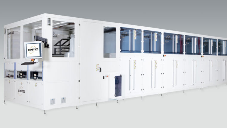
Kallisto Product Family
Electrochemical Deposition (ECD)
An advanced vertical processing platform for wet chemical treatment of substrates from 300x300mm up to Gen 5.1 (1100 x 1300mm) tailored to the needs of semi industry.
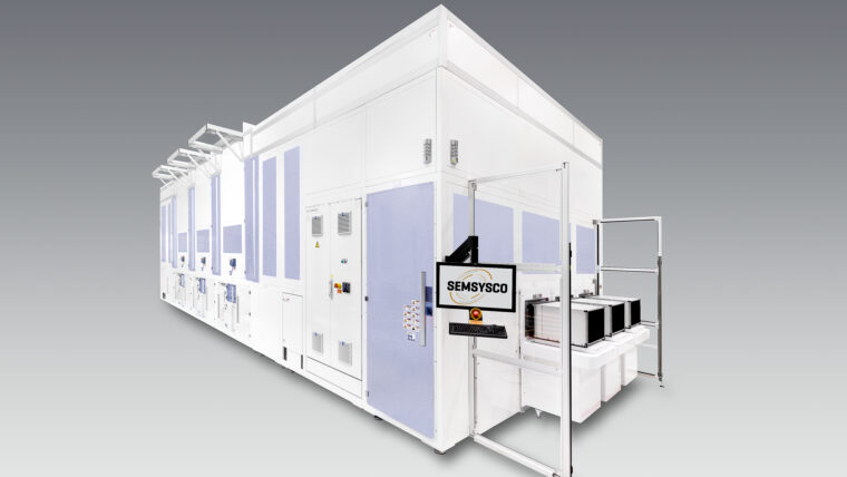
Phoenix Product Family
Electrochemical Deposition (ECD) PR-Development PR-Strip Wet Clean/Strip
Phoenix offers a fully-automated high volume panel processing for 510x515mm substrates.