
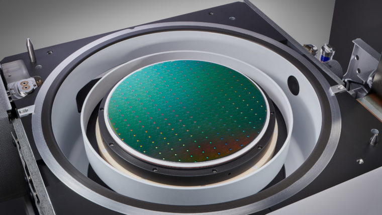
Memory cells – the chip components that store electronic data – include short-term volatile (such as DRAM) and long-term non-volatile (such as flash) storage types. DRAM is the mainstay for “working” (active) memory, while flash memory is used to store large amounts of data in a compact form.
To increase device density for more storage capacity, DRAM features continue to shrink, and NAND flash has moved to 3D architectures, which raise additional processing challenges. For example, the numerous layers in 3D NAND are vulnerable to stress, and any imperfections in the high aspect-ratio channels can create electrical shorts and interference. Production of newer memory types that bridge the gap between active and storage classes is also difficult due to the use of novel, hard-to-process materials. As a result, exceptional process control, flexibility, and productivity are needed.

By leading in innovation, Lam ensures our memory solutions meet the evolving demands of technology. One of the areas where we are innovating to meet the surge in demand for AI, VR, AR, and electric vehicles is our High Bandwidth Memory (HBM) technology. HBM embodies the future of high-performance computing with its 3D stacking and cutting-edge packaging, promising unparalleled performance and efficiency.
Facing the intricate challenges of advanced memory production, like hybrid bonding on-wafer performance and yield management, our expertise in micro-bumps and through-silicon vias (TSVs) equips us to deliver exceptional process control and productivity.
Advanced Memory
Our Solutions
ALTUS Product Family
Atomic Layer Deposition (ALD) Chemical Vapor Deposition (CVD)
Combining CVD and ALD technologies, these market-leading systems deposit highly conformal metal films for advanced tungsten metallization applications.

Coronus Product Family
Plasma Bevel Etch and Deposition
Coronus systems focus on the bevel edge to enhance overall yield. Semiconductor processing can cause residues and roughness to accumulate along the wafer edge where they may flake off, drift to other areas, and create defects that cause a device to fail. Coronus etch products remove bevel residues and Coronus deposition protect the wafer bevel from damage.
EOS Product Family
Wet Clean
Our advanced wet clean products deliver exceptionally low on-wafer defectivity at high throughput for progressively demanding applications.

Fabtex™ Yield Optimizer
Semiconductor Yield Optimization Platform
Fabtex™ Yield Optimizer is a cutting-edge software platform designed to help semiconductor foundries accelerate yield ramp and improve high-volume manufacturing performance.

Flex Product Family
Atomic Layer Etch (ALE) Cryogenic Etching Reactive Ion Etch (RIE)
Our dielectric etch systems offer application-focused capabilities for creating a wide range of challenging structures in advanced devices.
GAMMA Product Family
Dry Strip
These products provide the process flexibility needed to address a wide range of critical photoresist strip applications.
Kallisto Product Family
Electrochemical Deposition (ECD)
An advanced vertical processing platform for wet chemical treatment of substrates from 300x300mm up to Gen 5.1 (1100 x 1300mm) tailored to the needs of semi industry.

Kiyo Product Family
Reactive Ion Etch (RIE)
These market-leading conductor etch products deliver the high-performance precision and control at high productivity needed for critical device features.

Metior Product Family
Mass Metrology
Our mass metrology systems deliver sub-milligram measurement capability for advanced process monitoring and control of three-dimensional device structures.

OverViz
Plasma Modeling
OverViz™ is an industrial simulation software platform for high-fidelity modeling of plasma discharges.
Phoenix Product Family
Electrochemical Deposition (ECD) PR-Development PR-Strip Wet Clean/Strip
Phoenix offers a fully-automated high volume panel processing for 510x515mm substrates.
Reliant Deposition Products
Chemical Vapor Deposition (CVD) High-Density Plasma Chemical Vapor Deposition (HDP-CVD) Plasma-Enhanced Chemical Vapor Deposition (PECVD) Pulsed Laser Deposition (PLD) Reliant Systems
Our Reliant deposition products enable roadmaps for Specialty Technologies and extend the productive life of fabs.
Reliant Etch Products
Deep Reactive Ion Etch (DRIE) Reactive Ion Etch (RIE) Reliant Systems
Our Reliant etch products enable roadmaps for Specialty Technologies and extend the productive life of fabs.
SABRE Product Family
Electrochemical Deposition (ECD)
This product family offers precision metal plating for copper damascene manufacturing on the industry’s productivity-leading ECD platform.
Selective Etch Product Family
Selective Etch
Breakthrough portfolio delivers isotropic material removal with angstrom-scale precision and ultra-high selectivity capabilities for 3D architectures and advanced logic and foundry applications.
SEMulator3D
Semiconductor Process Modeling
SEMulator3D® is a semiconductor process modeling platform that offers wide ranging technology development capabilities.
Sense.i Product Family
Reactive Ion Etch (RIE)
Our latest etch platform offers unparalleled system intelligence in a compact, high-density architecture to deliver process performance at the highest productivity.
SPEED Product Family
High-Density Plasma Chemical Vapor Deposition (HDP-CVD)
These dielectric deposition products provide complete gapfill of high aspect ratio spaces with industry-leading throughput and reliability.
Striker Product Family
Atomic Layer Deposition (ALD)
Using advanced ALD technology, these products deliver dielectric films with exceptional control for critical processes in advanced devices with nanoscale features.
Syndion Product Family
Deep Reactive Ion Etch (DRIE) Reactive Ion Etch (RIE)
For deep etch applications, this product family provides the exceptional across-wafer uniformity control needed for critical high aspect ratio features.
Triton Product Family
Electrochemical Deposition (ECD) Wet Clean/Strip
The Triton platform is a versatile and modular solution for single wafer plating and wet processing.
Vantex Product Family
Cryogenic Etching Reactive Ion Etch (RIE)
Designed for the Sense.i platform, Vantex redefines high aspect ratio etching with innovations in technology and Equipment Intelligence.

VECTOR Product Family
Plasma-Enhanced Chemical Vapor Deposition (PECVD)
Our PECVD product family provides precise dielectric film deposition at high productivity for a wide range of device applications.
Versys Metal Product Family
Reactive Ion Etch (RIE)
These metal etch products provide excellent process control at high-productivity for electrical connection and metal hardmask applications.
Related Blog Posts
-

The Road to the AI Era Is Paved in Semiconductor Manufacturing Innovation
Jun 24, 2024“The Road to the AI Era Is Paved in Semiconductor Manufacturing Innovation," an in-depth white paper written by The TechArena and sponsored by Lam Research, explores the pivotal role of chipmaking innovation in ushering in the next transformative technological age. The paper provides authoritative insights into the revolutionary effects of generative AI and large language models across various industries, the emerging challenges in delivering performance to meet these advanced requirements, and the critical importance of high bandwidth memory (HBM) in AI compute platforms.
-
Will HBM Redefine What's Possible With AI?
Mar 19, 2024There is a lot of buzz around high bandwidth memory (HBM). As artificial intelligence (AI) continues to advance so do its demands. Many major technology companies are betting on HBM to meet them. HBM is an advanced computer memory designed to offer faster data access with lower energy consumption. For AI, it can be a critical component in performance and reducing power consumption in memory chips.