Products
Metior Product Family
Mass Metrology
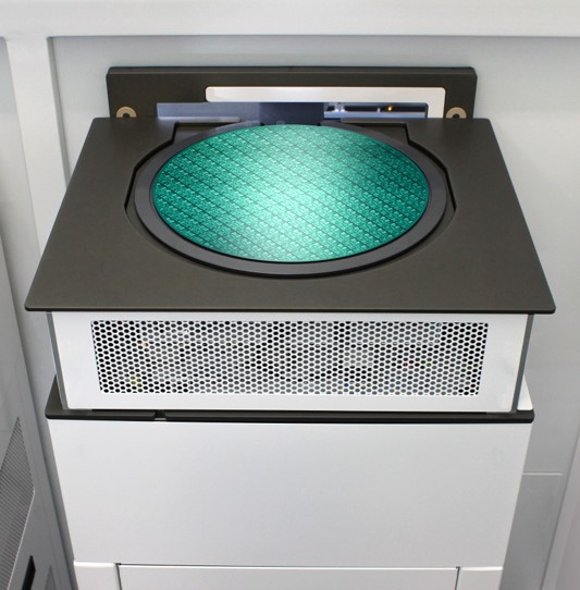
In-line process monitoring is used to identify production wafer trends and excursions as they occur, allowing corrections to be implemented quickly to prevent further yield loss. For deposition, etch, and clean steps, measurement of the mass change of a wafer before and after a process is a simple and direct means of monitoring and controlling process results, particularly for ultra-thin films, ultra-thick films, and complex 3D geometries of newer chip designs, where traditional optical metrology techniques are ineffective.
Lam’s Metior® mass metrology systems, available as both platform-integrated modules and as stand-alone systems, deliver sub-milligram mass measurement capability for advanced process monitoring and control of three-dimensional device structures.
As devices become more three-dimensionally complex, traditional optical metrology techniques are often insufficient for maintaining tight control of etch, deposition, and clean processes. For example, the bottoms of high aspect ratio (HAR) structures may be invisible to top-down optical signals. Likewise, certain thick films are frequently too opaque for precise thickness measurement, and lateral processing steps occur too deeply in a structure to be visible. Many geometries are now so complex that fitting optical critical dimension (OCD) models requires substantial investment and long development and validation timelines. In addition, meeting tight requirements for etch applications often requires real-time methods for addressing within-lot and lot-to-lot variability sources. As a result, chipmakers require an alternative means of monitoring process results that addresses the limitations of optical techniques in a cost-effective manner.