Enabling chipmakers to create the future
Advanced microchips are in many of the familiar products we use every day – from mobile phones and computing devices to entertainment systems and increasingly “smart” cars. Electronic products are everywhere and life without them is unimaginable.
Creating the tiny, complex chips used in these devices involves the repetition of a core set of processes and includes hundreds of individual steps. For successful production, semiconductor manufacturers require sophisticated processes and fabrication equipment.
We work closely with customers to deliver the products and technologies needed to enable their success. By offering critical chip-processing capabilities, our products provide a vital link between the visionary designs for the latest electronic devices and the companies that produce them.
Akara®
Designed for high-volume production with maximum process yield, Akara® increases wafer output and eliminates wasted time, with millisecond response times to any change. The industry’s most advanced etch uniformity controls provide angstrom-level critical dimension uniformity and wafer to wafer repeatability.

ALTUS Product Family
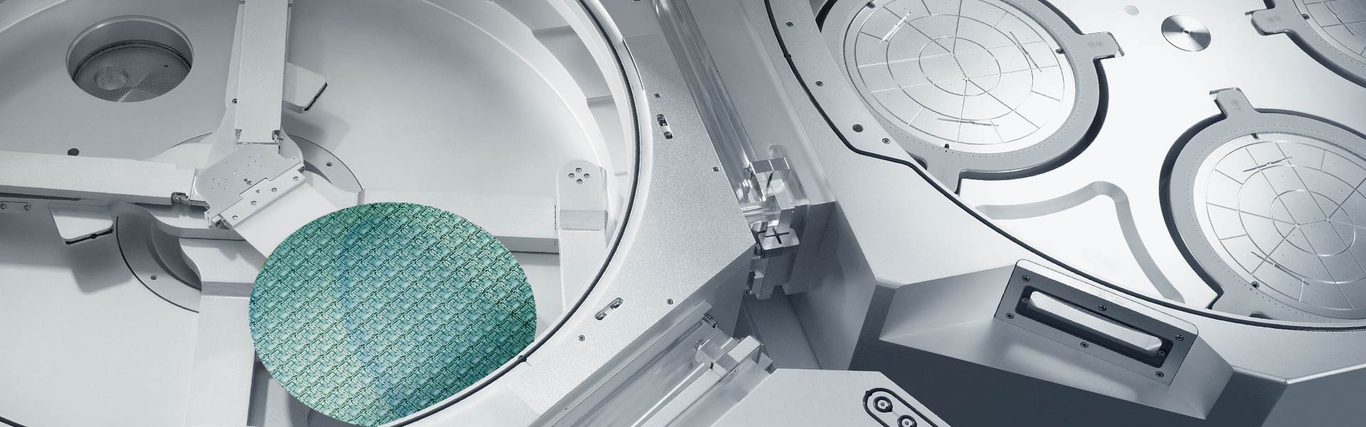
Combining CVD and ALD technologies, these market-leading systems deposit highly conformal metal films for advanced tungsten metallization applications.
Coronus Product Family
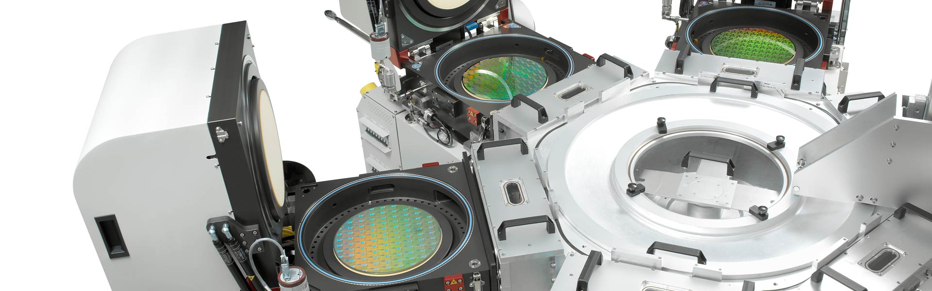
Coronus systems focus on the bevel edge to enhance overall yield. Semiconductor processing can cause residues and roughness to accumulate along the wafer edge where they may flake off, drift to other areas, and create defects that cause a device to fail. Coronus etch products remove bevel residues and Coronus deposition protect the wafer bevel from damage.
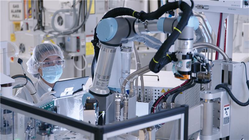
Dextro™
Dextro is a mobile unit with a robotic arm and uses various end-effectors as hands to manage critical equipment maintenance tasks that are time-consuming and prone to errors when done manually. Operated by a fab technician or engineer, Dextro executes complex maintenance tasks with precision and repeatability that are beyond human capability alone, enabling higher tool uptime and manufacturing yield.
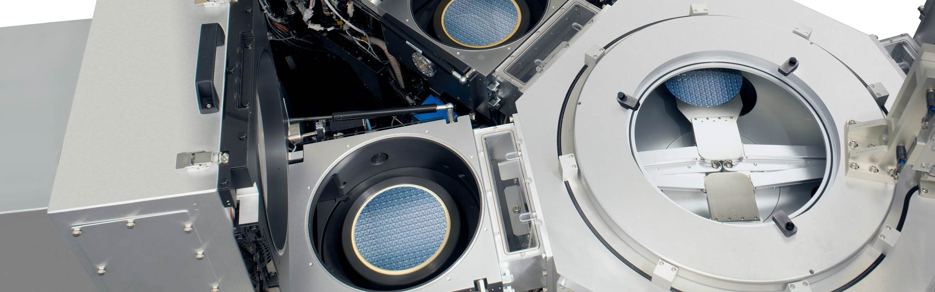
DSiE Product Family
These products deliver exceptional process control at high productivity for several critical and non-critical deep silicon etch applications.
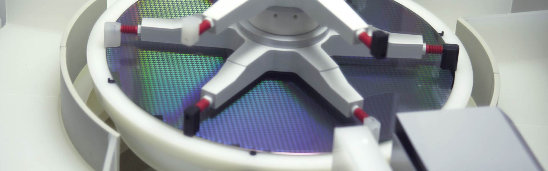
DV-Prime & Da Vinci Product Families
These products provide the process flexibility needed with high productivity to address multiple wafer cleaning steps throughout manufacturing.
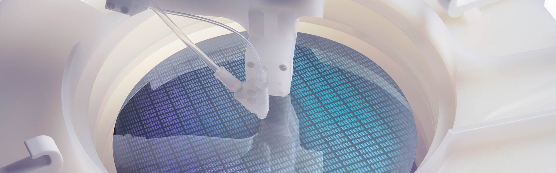
EOS Product Family
Our advanced wet clean products deliver exceptionally low on-wafer defectivity at high throughput for progressively demanding applications.

Fabtex™ Yield Optimizer
Fabtex™ Yield Optimizer is a cutting-edge software platform designed to help semiconductor foundries accelerate yield ramp and improve high-volume manufacturing performance.
Flex Product Family
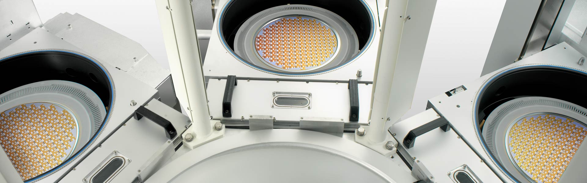
Our dielectric etch systems offer application-focused capabilities for creating a wide range of challenging structures in advanced devices.
GAMMA Product Family
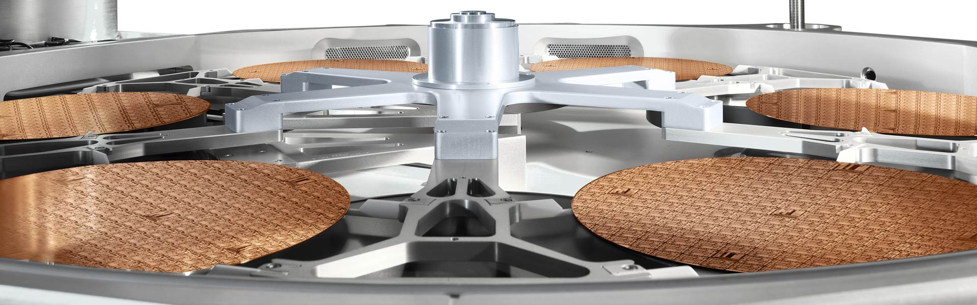
These products provide the process flexibility needed to address a wide range of critical photoresist strip applications.
Kallisto Product Family
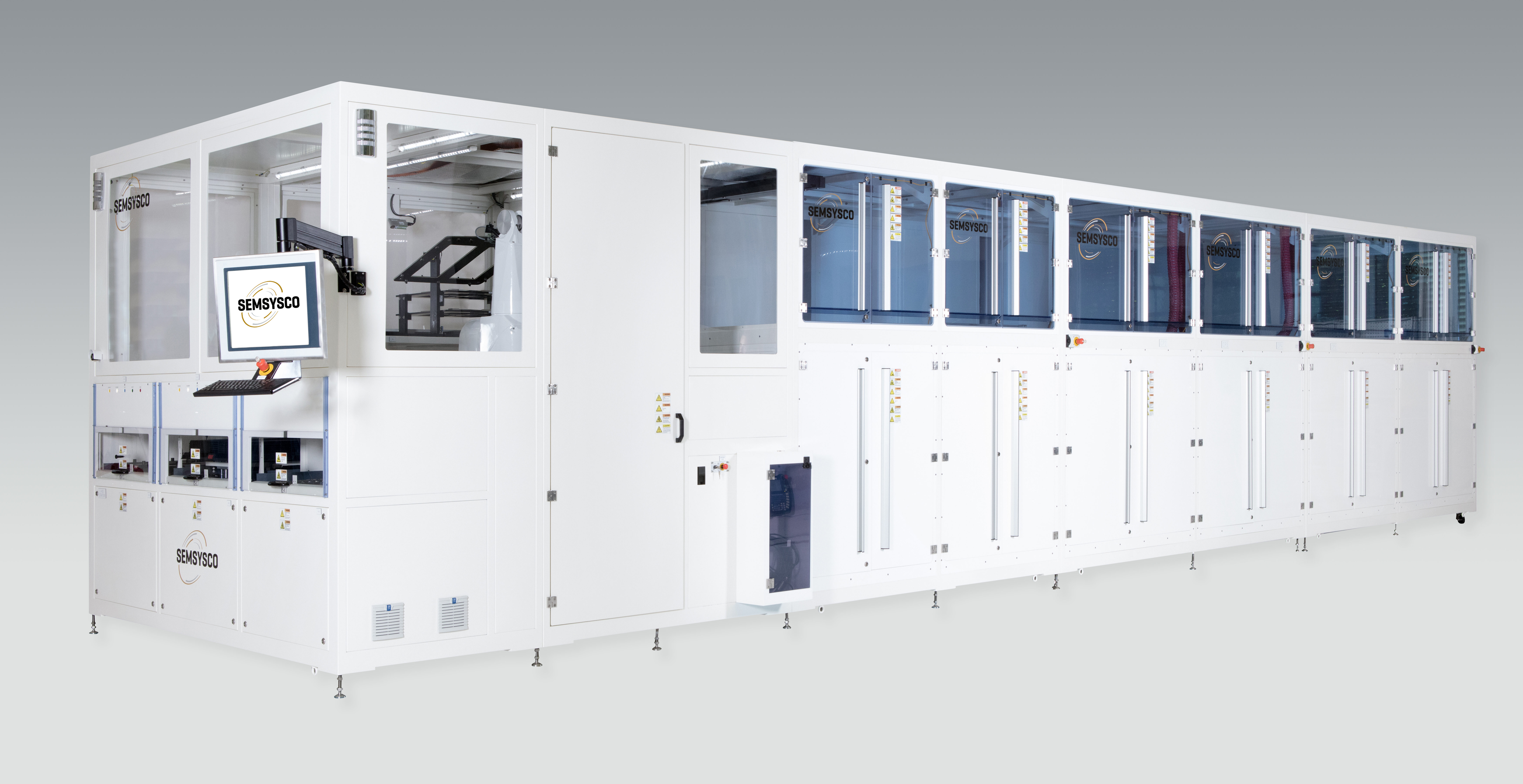
An advanced vertical processing platform for wet chemical treatment of substrates from 300x300mm up to Gen 5.1 (1100 x 1300mm) tailored to the needs of semi industry.
Kiyo Product Family
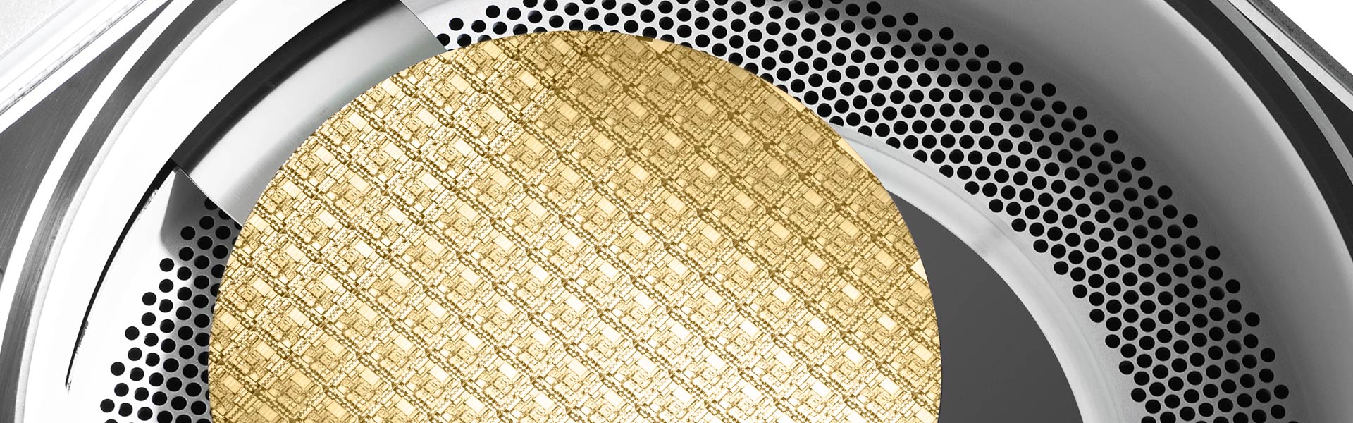
These market-leading conductor etch products deliver the high-performance precision and control at high productivity needed for critical device features.
Metior Product Family
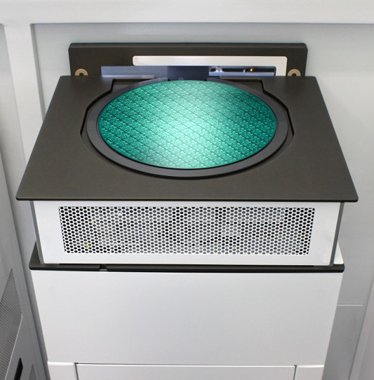
Our mass metrology systems deliver sub-milligram measurement capability for advanced process monitoring and control of three-dimensional device structures.

OverViz
OverViz™ is an industrial simulation software platform for high-fidelity modeling of plasma discharges.
Phoenix Product Family
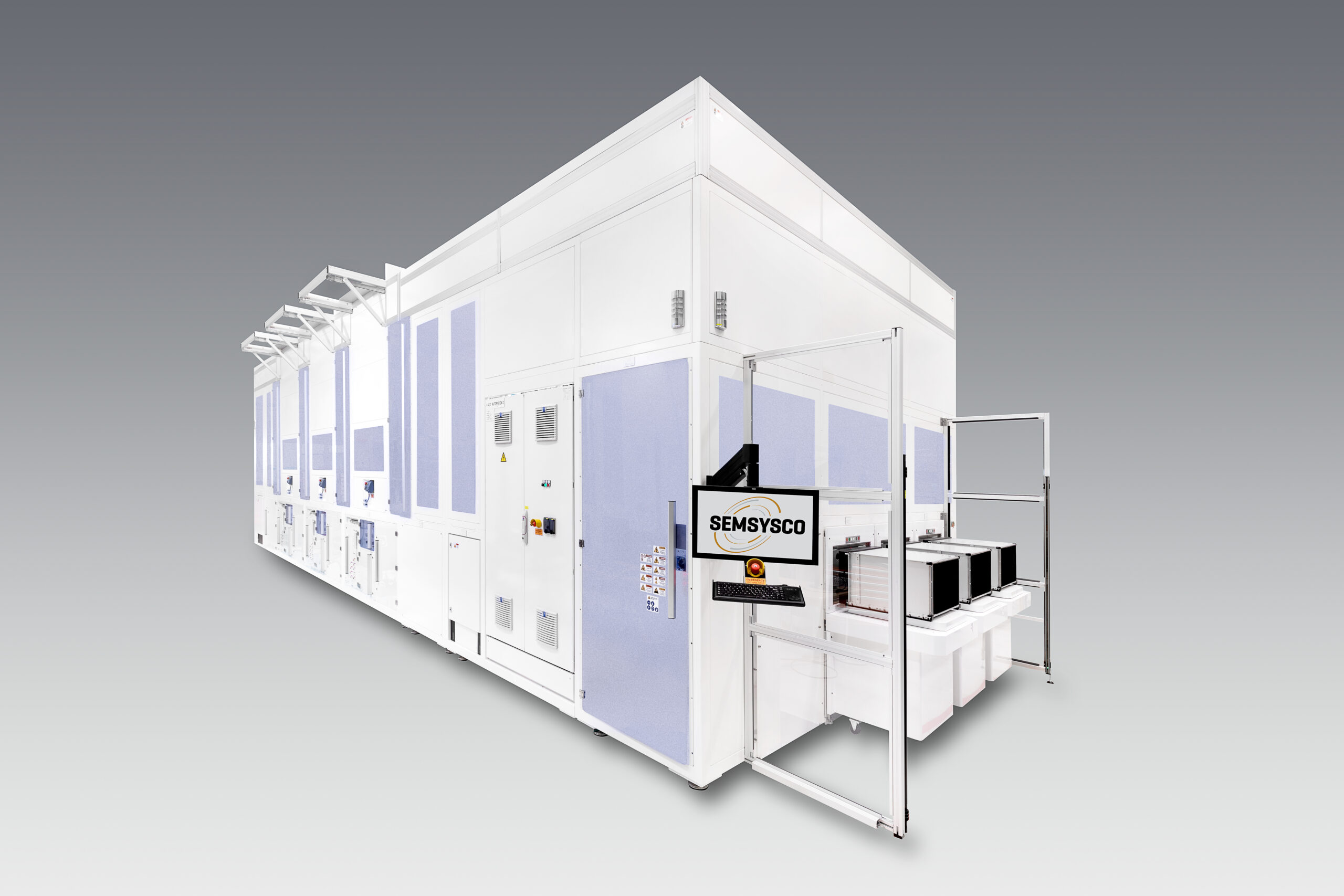
Phoenix offers a fully-automated high volume panel processing for 510x515mm substrates.
Prestis™
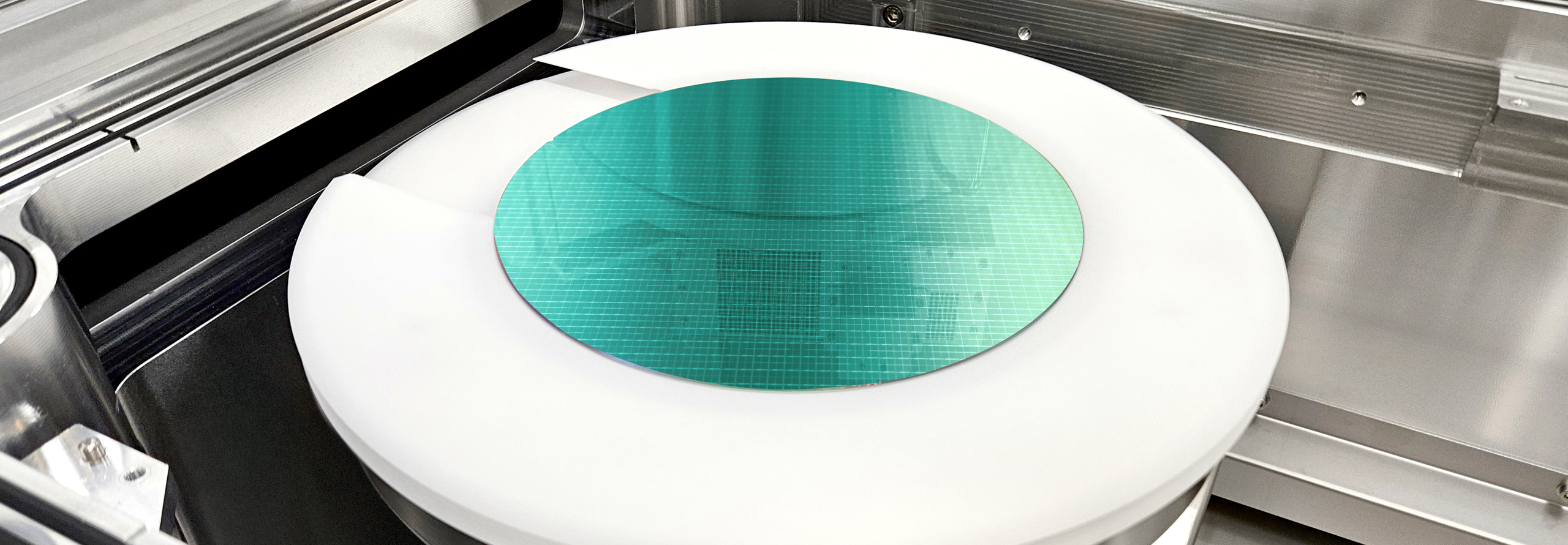
Our Prestis™ product provides thin film deposition solutions for a wide range of complex multi-element materials for Specialty Technologies applications.
Reliant Clean Products
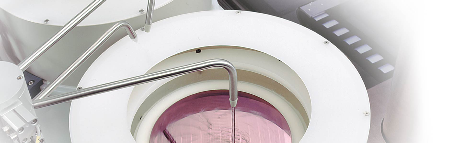
Our Reliant clean products enable roadmaps for Specialty Technologies and extend the productive life of fabs.
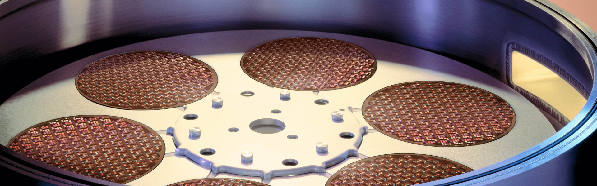
Reliant Deposition Products
Our Reliant deposition products enable roadmaps for Specialty Technologies and extend the productive life of fabs.
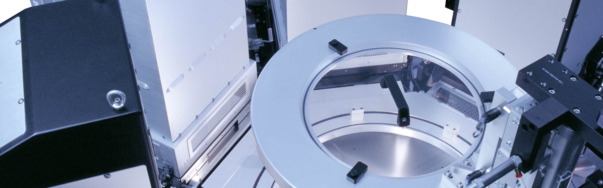
Reliant Etch Products
Our Reliant etch products enable roadmaps for Specialty Technologies and extend the productive life of fabs.
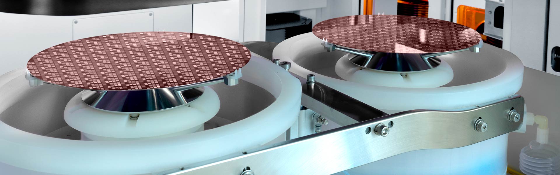
SABRE 3D Product Family
Using our proven Electrofill technology, these high-productivity systems deliver quality metal films for advanced packaging applications.
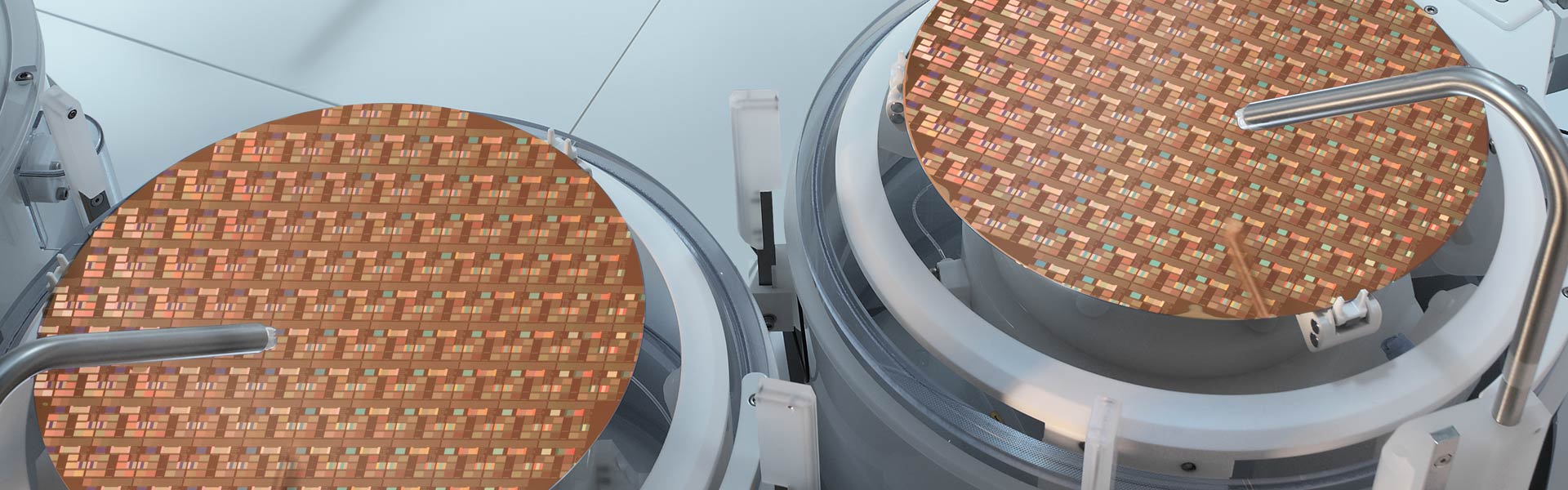
SABRE Product Family
This product family offers precision metal plating for copper damascene manufacturing on the industry’s productivity-leading ECD platform.
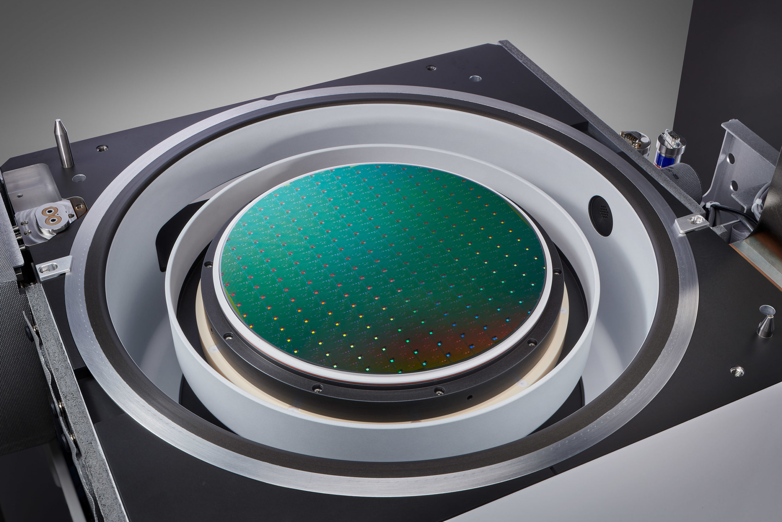
Selective Etch Product Family
Breakthrough portfolio delivers isotropic material removal with angstrom-scale precision and ultra-high selectivity capabilities for 3D architectures and advanced logic and foundry applications.

Semiverse® Solutions
Our semiconductor process modeling software, SEMulator3D®, performs predictive modeling of etch, deposition & other integrated processes, to identify problems prior to fabrication. VizGlow™ is a simulation platform for high-fidelity modeling of non-equilibrium plasma discharges.
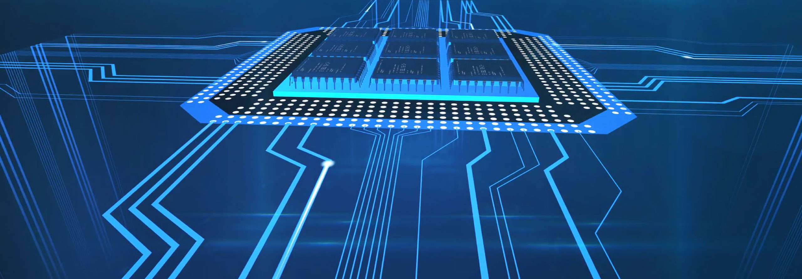
SEMulator3D
SEMulator3D® is a semiconductor process modeling platform that offers wide ranging technology development capabilities.
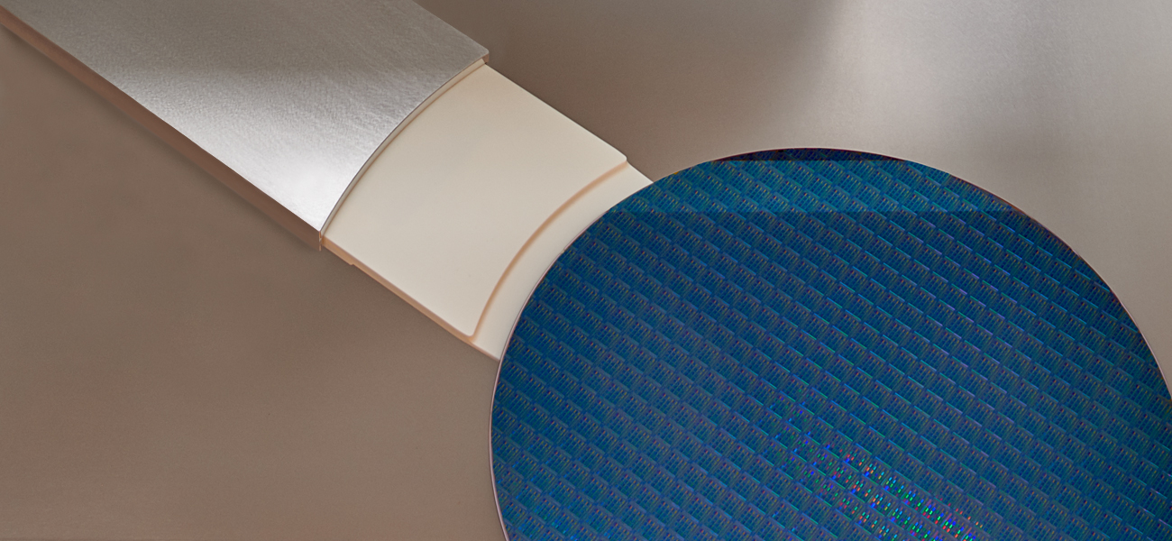
Sense.i Product Family
Our latest etch platform offers unparalleled system intelligence in a compact, high-density architecture to deliver process performance at the highest productivity.
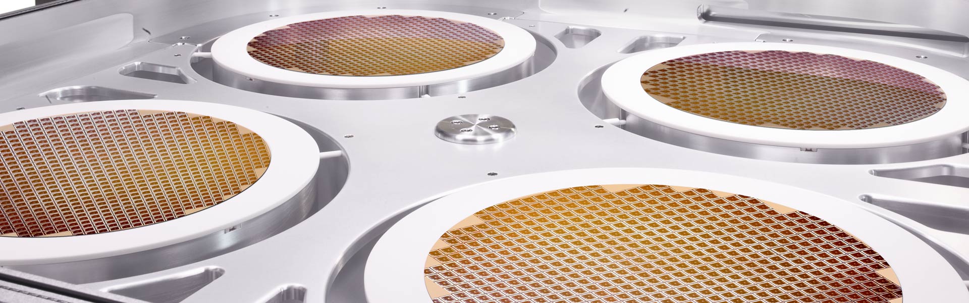
SOLA Product Family
This product family offers specialized post-deposition film treatments to improve physical characteristics for advanced film applications.
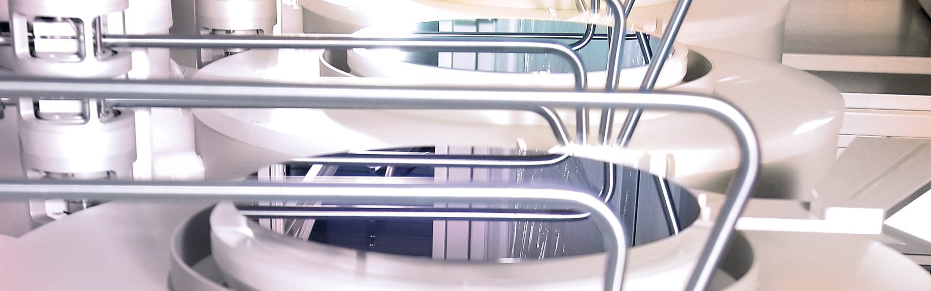
SP Series Product Family
This proven product family delivers reliable, cost-efficient wet clean/wet etch solutions that gently remove unwanted materials from the wafer.
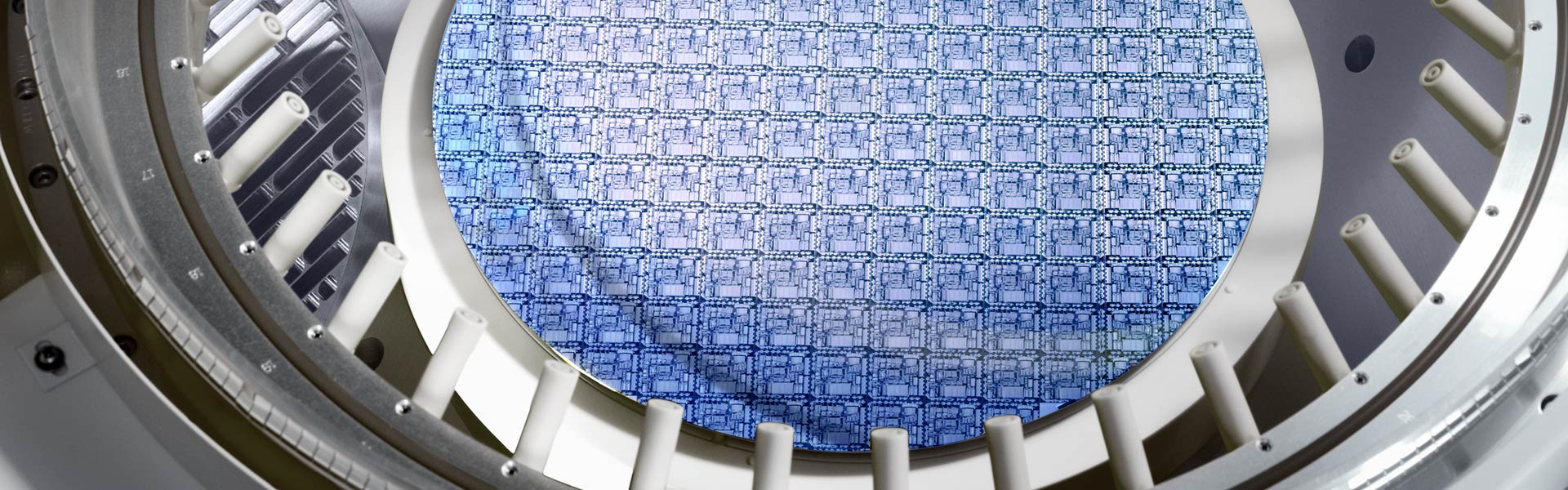
SPEED Product Family
These dielectric deposition products provide complete gapfill of high aspect ratio spaces with industry-leading throughput and reliability.
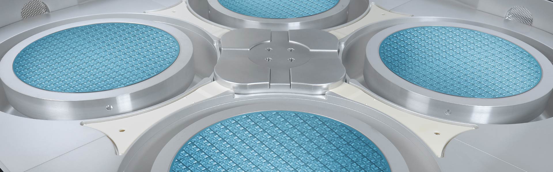
Striker Product Family
Using advanced ALD technology, these products deliver dielectric films with exceptional control for critical processes in advanced devices with nanoscale features.
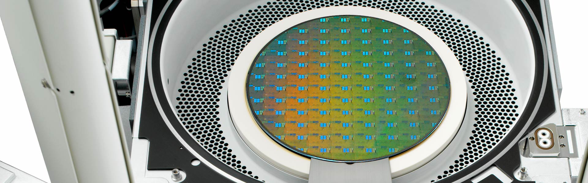
Syndion Product Family
For deep etch applications, this product family provides the exceptional across-wafer uniformity control needed for critical high aspect ratio features.
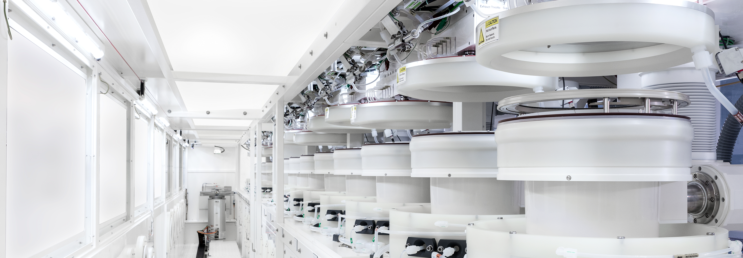
Triton Product Family
The Triton platform is a versatile and modular solution for single wafer plating and wet processing.
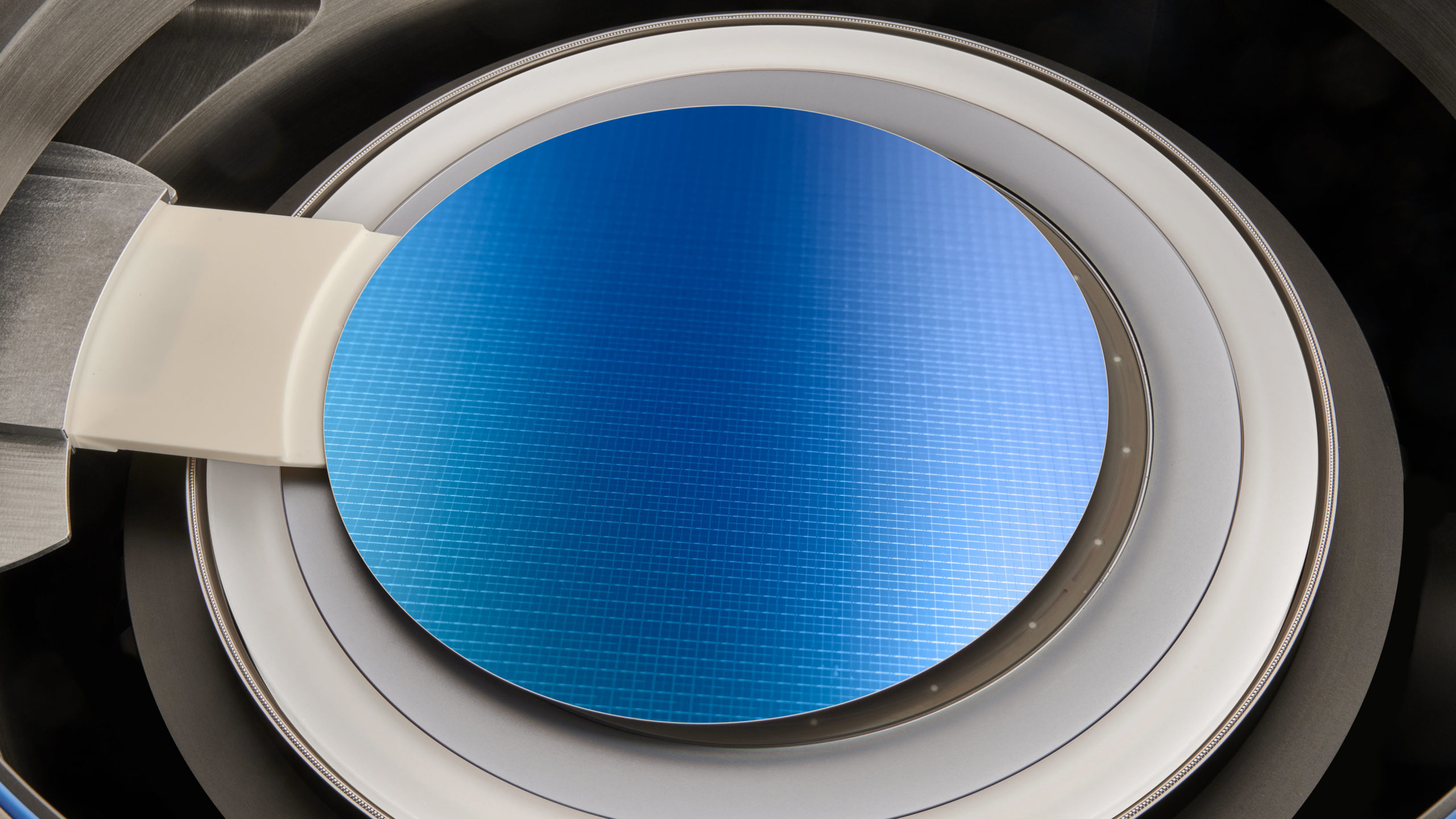
Vantex Product Family
Designed for the Sense.i platform, Vantex redefines high aspect ratio etching with innovations in technology and Equipment Intelligence.
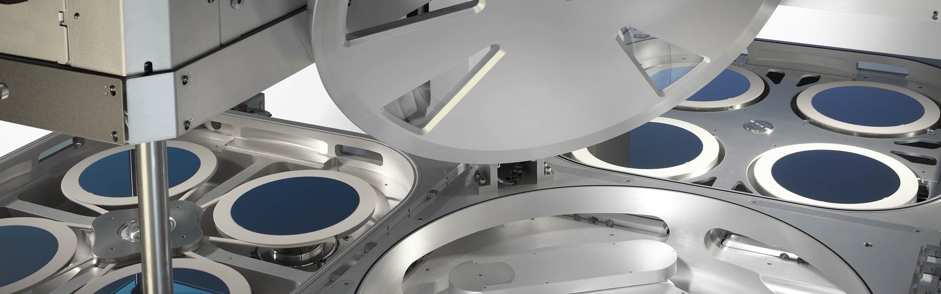
VECTOR Product Family
Our PECVD product family provides precise dielectric film deposition at high productivity for a wide range of device applications.
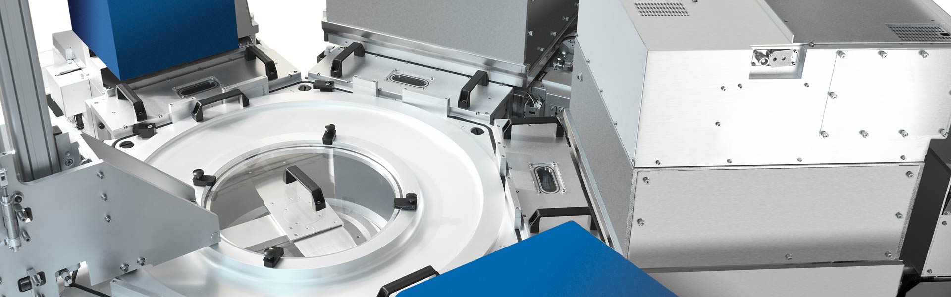
Versys Metal Product Family
These metal etch products provide excellent process control at high-productivity for electrical connection and metal hardmask applications.