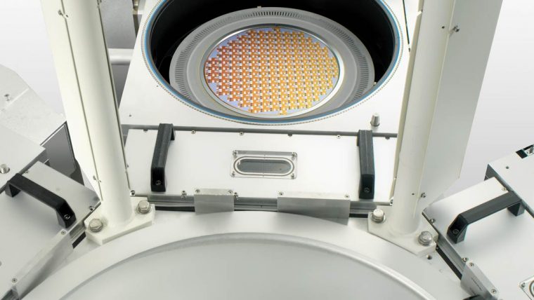
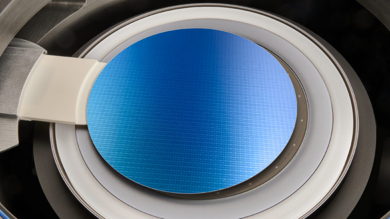
With today’s data-intensive AI applications require significant advancements in memory technology—particularly in NAND flash memory, including faster data transfer speeds. The surge in compute demand leads to an increase in power consumption to handle data transfers within memory systems. Chipmakers need to scale from 200 layers of 3D NAND and beyond to meet cost per bit reductions while reducing environmental impacts.
Low temperature, cryogenic etching enables the use of new, novel chemistries to deliver increased high aspect ratio etch capability. Cryogenic delivers enhanced etch rates, vertical high aspect ratio profiles, and reduces the environmental impact of the etching process.
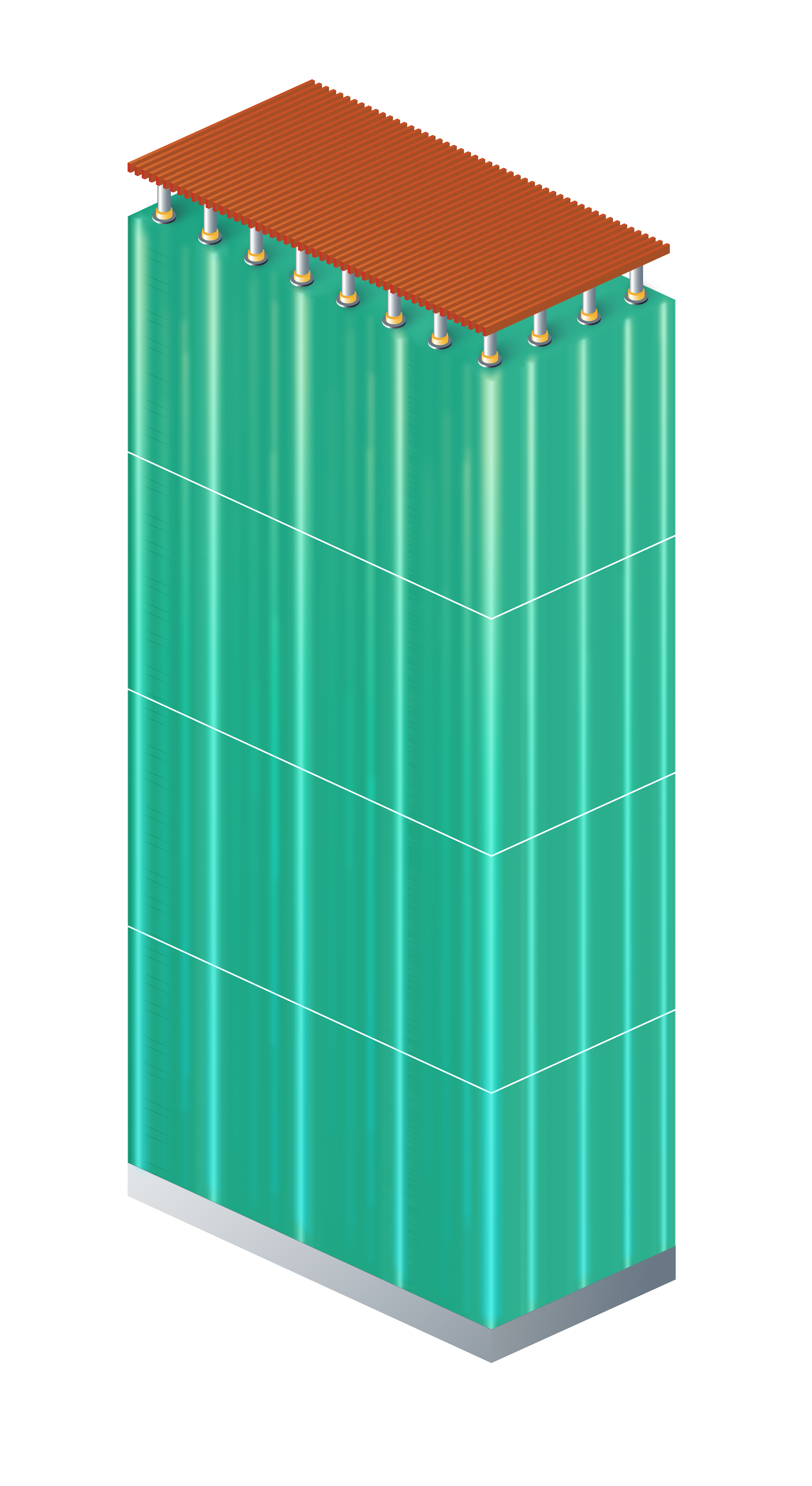
Through the use of proprietary and unique technologies, Lam has perfected the channel hole etching over time with:
- Cryogenic high aspect ratio etching: Uniform deep etch enables more bits per cell
- Wordline pitch scaling: Thinner oxide/nitride deposition layers enable more bits per device VECTOR® PECVD (high productivity oxide gap fill) and ALTUS® W (HAR tungsten fill with low stress)
- Advanced wordline metallization: Lower resistance metal enables thinner connections and faster device. VECTOR® Strata® (uniform Ox/SiN layer control with low stress), Kiyo®, Halo (void-free Mo fill in HAR features)
- Wafer stress management: Backside deposition controls wafer bow and enables taller device. Coronus® DX (high selectivity bevel film dep), VECTOR® DT (uniform backside film for wafer bow compensation) and EOS® (high productivity backside film etch)
With these technologies, Lam has enabled our customers to achieve near-perfect memory hole etch profiles with high throughput and low environmental impact.
Introducing Lam Cryo™ 3.0
Lam Cryo™ 3.0 allows for higher aspect ratio features with breakthrough precision and profile control. Leveraging innovations in surface chemistry, plasma physics, and process design, Lam’s Cryo™ 3.0 is optimized to manufacture future 3D NAND devices with 400 layers and beyond.
Lam Cryo™ 3.0 is compatible with Flex® and Vantex®, which all leading memory manufacturers use for the device-critical channel hole etch in high-volume 3D NAND production. Adding Lam Cryo™ 3.0 capability to existing and future installed base allows customers to maximize their equipment investment with exceptional performance and productivity.
Learn more about cryogenic etching and evolving 3D innovations here.
The Path to 1,000-layer 3D NAND
Storage memory in the AI eraCryogenic Etching
Related ProductsLam’s cryogenic dielectric etch technology is compatible with Lam’s popular Flex® dielectric etch technology and Vantex® reactive ion etch systems on the Sense.i® platform – enabling customers to easily leverage and expand on investment in their existing infrastructure.
Flex Product Family
Atomic Layer Etch (ALE) Cryogenic Etching Reactive Ion Etch (RIE)
Our dielectric etch systems offer application-focused capabilities for creating a wide range of challenging structures in advanced devices.
Vantex Product Family
Cryogenic Etching Reactive Ion Etch (RIE)
Designed for the Sense.i platform, Vantex redefines high aspect ratio etching with innovations in technology and Equipment Intelligence.
Additional Resources
-
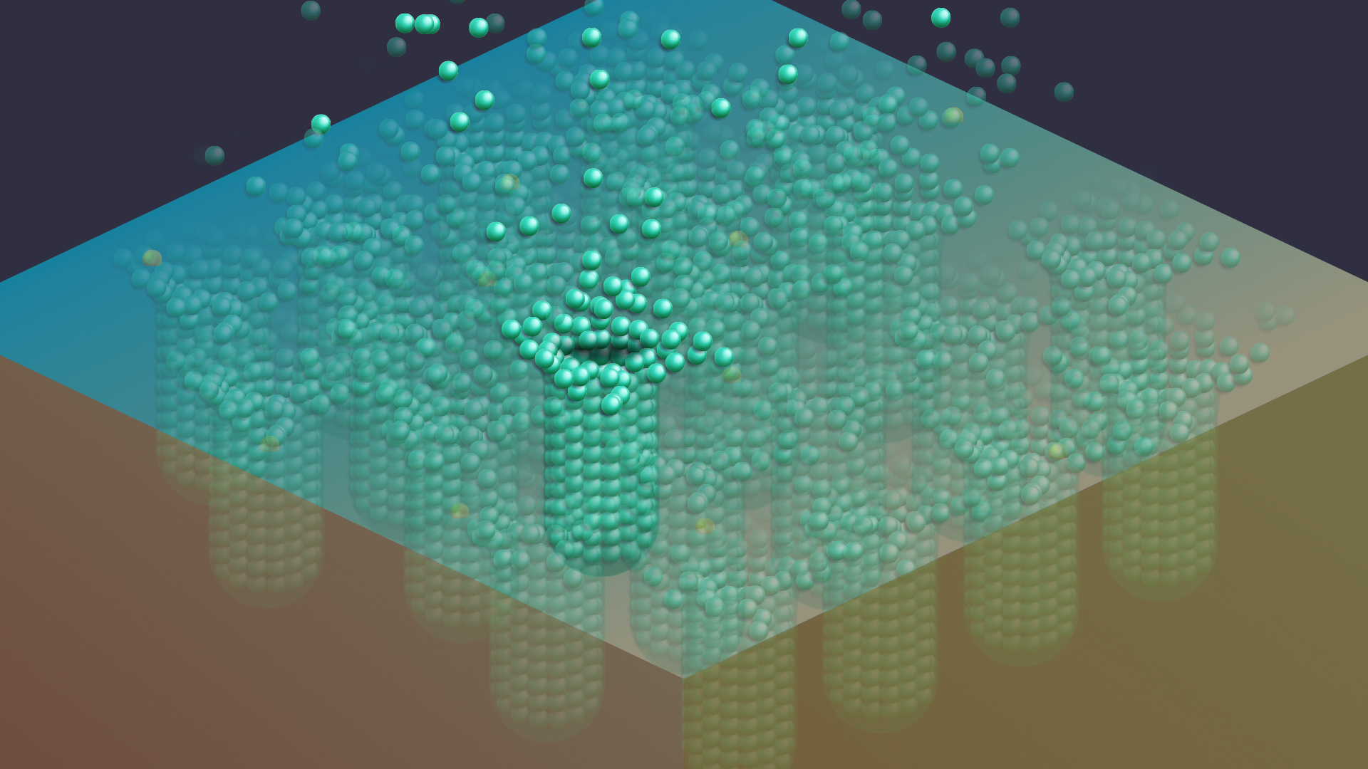
Introducing Lam Cryogenic Etching
-
Scaling to 1,000-Layer NAND in the AI Era
