
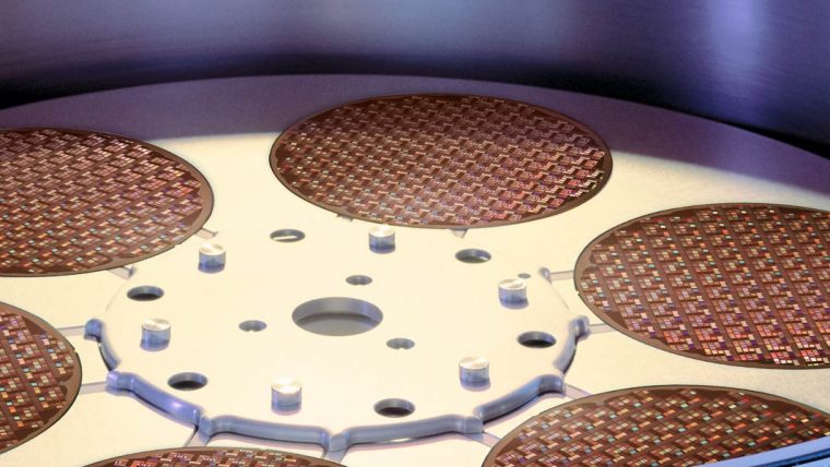
Patterning involves the set of process steps – including lithography, deposition, and etch – that create the extremely small, intricate features of an integrated circuit. With each new generation, device dimensions continue to shrink. For advanced structures, these feature sizes can be too small and/or packed too closely together for conventional lithography, the step that transfers the chip design’s intricate detail from the mask “template” onto the wafer. To compensate, chipmakers are using advanced techniques like double/quadruple and spacer-based patterning, involving multiple masks and process sets. Even as these approaches ease lithography limitations, they create new demands for exceptional process precision and film quality in order to accurately produce the fine, dense features required.
Patterning
Our Solutions
Coronus Product Family
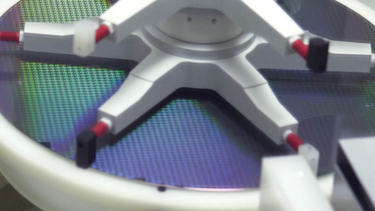
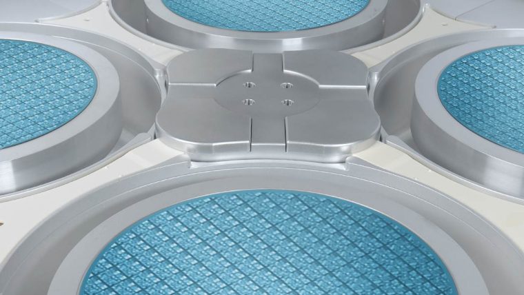
Plasma Bevel Etch and Deposition
Coronus systems focus on the bevel edge to enhance overall yield. Semiconductor processing can cause residues and roughness to accumulate along the wafer edge where they may flake off, drift to other areas, and create defects that cause a device to fail. Coronus etch products remove bevel residues and Coronus deposition protect the wafer bevel from damage.
DV-Prime & Da Vinci Product Families
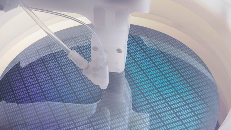
Wet Clean
These products provide the process flexibility needed with high productivity to address multiple wafer cleaning steps throughout manufacturing.
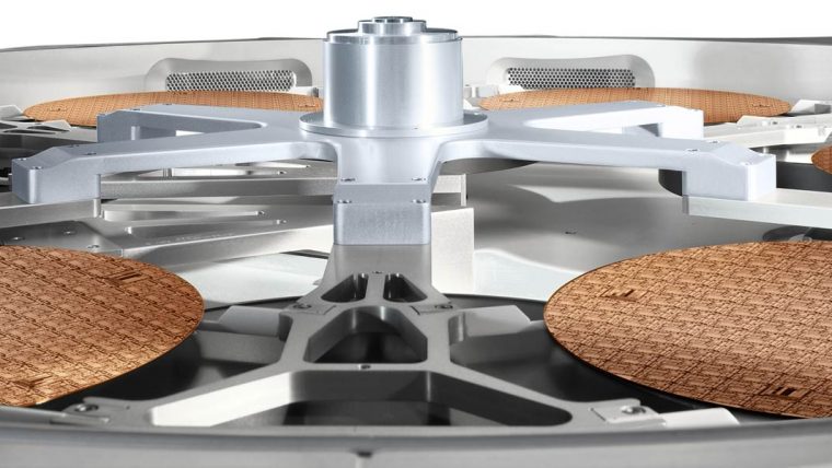
EOS Product Family
Wet Clean
Our advanced wet clean products deliver exceptionally low on-wafer defectivity at high throughput for progressively demanding applications.

Fabtex™ Yield Optimizer
Semiconductor Yield Optimization Platform
Fabtex™ Yield Optimizer is a cutting-edge software platform designed to help semiconductor foundries accelerate yield ramp and improve high-volume manufacturing performance.

Flex Product Family
Atomic Layer Etch (ALE) Cryogenic Etching Reactive Ion Etch (RIE)
Our dielectric etch systems offer application-focused capabilities for creating a wide range of challenging structures in advanced devices.
GAMMA Product Family
Dry Strip
These products provide the process flexibility needed to address a wide range of critical photoresist strip applications.

Kiyo Product Family
Reactive Ion Etch (RIE)
These market-leading conductor etch products deliver the high-performance precision and control at high productivity needed for critical device features.

Metior Product Family
Mass Metrology
Our mass metrology systems deliver sub-milligram measurement capability for advanced process monitoring and control of three-dimensional device structures.
Reliant Clean Products
Reliant Systems Wet Clean/Strip
Our Reliant clean products enable roadmaps for Specialty Technologies and extend the productive life of fabs.
Reliant Deposition Products
Chemical Vapor Deposition (CVD) High-Density Plasma Chemical Vapor Deposition (HDP-CVD) Plasma-Enhanced Chemical Vapor Deposition (PECVD) Pulsed Laser Deposition (PLD) Reliant Systems
Our Reliant deposition products enable roadmaps for Specialty Technologies and extend the productive life of fabs.
Selective Etch Product Family
Selective Etch
Breakthrough portfolio delivers isotropic material removal with angstrom-scale precision and ultra-high selectivity capabilities for 3D architectures and advanced logic and foundry applications.
SEMulator3D
Semiconductor Process Modeling
SEMulator3D® is a semiconductor process modeling platform that offers wide ranging technology development capabilities.
Sense.i Product Family
Reactive Ion Etch (RIE)
Our latest etch platform offers unparalleled system intelligence in a compact, high-density architecture to deliver process performance at the highest productivity.
Striker Product Family
Atomic Layer Deposition (ALD)
Using advanced ALD technology, these products deliver dielectric films with exceptional control for critical processes in advanced devices with nanoscale features.

VECTOR Product Family
Plasma-Enhanced Chemical Vapor Deposition (PECVD)
Our PECVD product family provides precise dielectric film deposition at high productivity for a wide range of device applications.
Versys Metal Product Family
Reactive Ion Etch (RIE)
These metal etch products provide excellent process control at high-productivity for electrical connection and metal hardmask applications.
Related Blog Posts
-

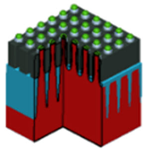
Improving Line Edge Roughness Using Virtual Fabrication
May 28, 2024Line edge roughness (LER) is a variation in the width of a lithographic pattern along one edge of a structure inside a chip. Line edge roughness can be a critical variation source and defect mechanism in advanced logic and memory devices, and can lead to poor device performance or even device failure [1~3]. Deposition-etch cycling is an effective technique to reduce line edge roughness. In this study, we demonstrate how virtual fabrication can provide guidance on how to perform deposition/etch cycling in order to reduce LER.
-
Virtual Exploration of Novel Vertical DRAM Architectures
Apr 16, 2024In this article, we demonstrate a pathfinding technique for a novel Vertical DRAM technology. First, we identify important process parameters (defined by current semiconductor production equipment capabilities) that strongly impact yield. By using a virtual model, we then perform experimental optimization of the Vertical DRAM device across specific target ranges, to help predict and improve the yield of this next generation product.