Creating flawless
thin films
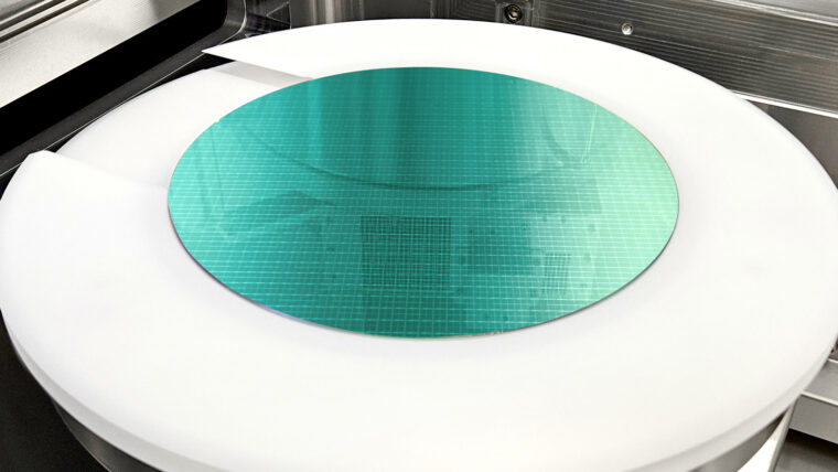
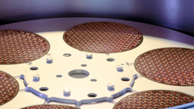
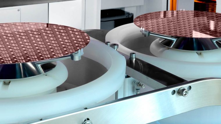
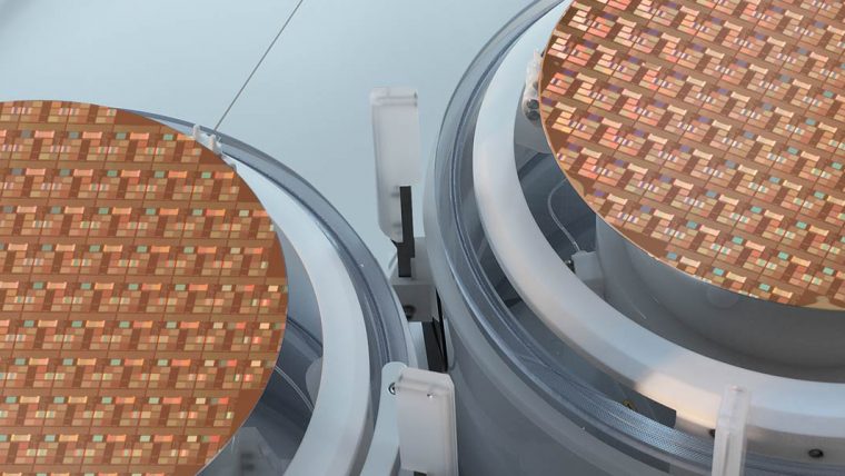
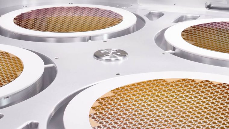
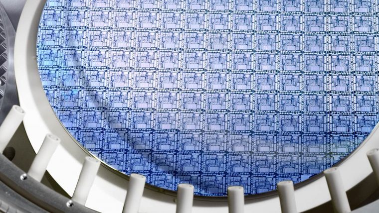
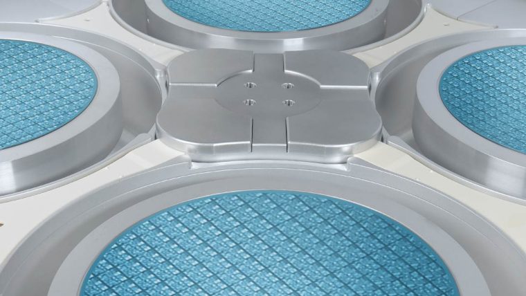
Deposition processes create layers of dielectric (insulating) and metal (conducting) materials used to build a semiconductor device. Depending on the type of material and structure being made, different techniques are employed. Electrochemical deposition (ECD) creates the copper “wiring” (interconnect) that links devices in an integrated circuit. Metal plating of copper and other metals is also used for through-silicon vias and wafer-level packaging applications. Tiny tungsten connectors and thin barriers are made with the precision of chemical vapor deposition (CVD) and atomic layer deposition (ALD), which adds only a few layers of atoms at a time. Plasma-enhanced CVD (PECVD), high-density plasma CVD (HDP-CVD), and ALD are used to form the critical insulating layers that isolate and protect all of these electrical structures. Pulsed laser deposition (PLD) is used to enable high performance piezoelectric layers. PLD is a physical vapor deposition method that uses high pulsed energy laser light to energize material, creating a deposition vapor that can be condensed on different substrates.
For the numerous materials and demanding features involved, Lam’s thin film deposition products provide the precision, performance, and flexibility needed for a wide range of challenging device applications.
Deposition
Our Products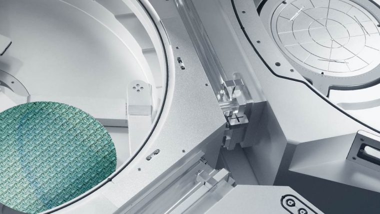
ALTUS Product Family
Atomic Layer Deposition (ALD) Chemical Vapor Deposition (CVD)
Combining CVD and ALD technologies, these market-leading systems deposit highly conformal metal films for advanced tungsten metallization applications.
Kallisto Product Family
Electrochemical Deposition (ECD)
An advanced vertical processing platform for wet chemical treatment of substrates from 300x300mm up to Gen 5.1 (1100 x 1300mm) tailored to the needs of semi industry.
Phoenix Product Family
Electrochemical Deposition (ECD) PR-Development PR-Strip Wet Clean/Strip
Phoenix offers a fully-automated high volume panel processing for 510x515mm substrates.
Prestis™
Pulsed Laser Deposition (PLD)
Our Prestis™ product provides thin film deposition solutions for a wide range of complex multi-element materials for Specialty Technologies applications.
Reliant Deposition Products
Chemical Vapor Deposition (CVD) High-Density Plasma Chemical Vapor Deposition (HDP-CVD) Plasma-Enhanced Chemical Vapor Deposition (PECVD) Pulsed Laser Deposition (PLD) Reliant Systems
Our Reliant deposition products enable roadmaps for Specialty Technologies and extend the productive life of fabs.
SABRE 3D Product Family
Electrochemical Deposition (ECD)
Using our proven Electrofill technology, these high-productivity systems deliver quality metal films for advanced packaging applications.
SABRE Product Family
Electrochemical Deposition (ECD)
This product family offers precision metal plating for copper damascene manufacturing on the industry’s productivity-leading ECD platform.
SOLA Product Family
Ultraviolet Thermal Processing (UVTP)
This product family offers specialized post-deposition film treatments to improve physical characteristics for advanced film applications.
SPEED Product Family
High-Density Plasma Chemical Vapor Deposition (HDP-CVD)
These dielectric deposition products provide complete gapfill of high aspect ratio spaces with industry-leading throughput and reliability.
Striker Product Family
Atomic Layer Deposition (ALD)
Using advanced ALD technology, these products deliver dielectric films with exceptional control for critical processes in advanced devices with nanoscale features.
Triton Product Family
Electrochemical Deposition (ECD) Wet Clean/Strip
The Triton platform is a versatile and modular solution for single wafer plating and wet processing.

VECTOR Product Family
Plasma-Enhanced Chemical Vapor Deposition (PECVD)
Our PECVD product family provides precise dielectric film deposition at high productivity for a wide range of device applications.
Related blog posts
-
Lam’s Laser Focus on the Future of Chip Manufacturing
Mar 26, 2024Lam Research hopes to revolutionize microchip manufacturing with the launch of a new system: Prestis™. Why it matters: For the first time in semiconductor production, Lam is using lasers to deposit thin films and bringing pulsed laser deposition (PLD) to wafer-level mass production. Prestis is expected to be key in developing cutting-edge specialty technologies devices, such as RF (radio frequency) filters for 5G and Wi-Fi 6 and high-end MEMS (micro-electromechanical systems) microphones.
-
Introducing Coronus DX, World’s First Bevel Deposition Solution Optimized for 3D Chipmaking
Jun 20, 2023For more than 15 years, Lam’s Coronus® product family has been the leader in wafer bevel technology. Today we introduced the newest member of the family, Coronus DX. It’s the industry’s first bevel deposition solution optimized to tackle key manufacturing challenges in next-gen logic, 3D NAND and advanced packaging applications.