Products
Triton Product Family
Electrochemical Deposition (ECD)Wet Clean/Strip
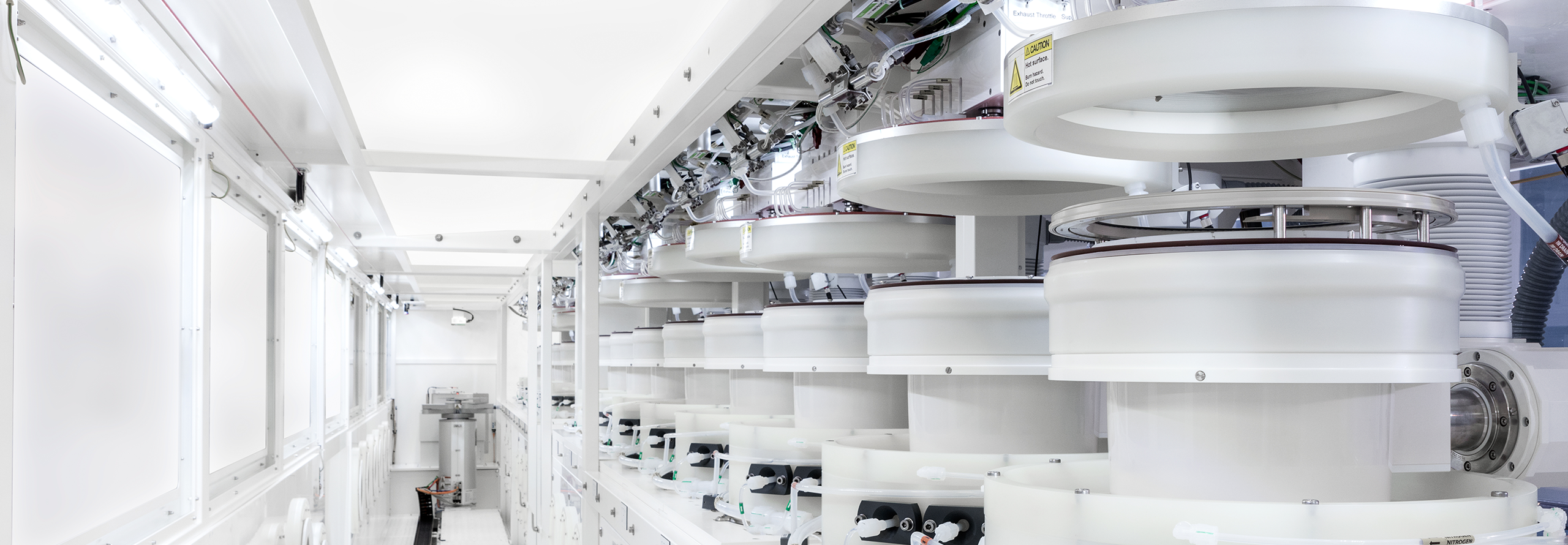
The Triton platform is a versatile and modular solution for single wafer plating and wet processing. Its design makes this system the first choice for R&D and is expandable to support high volume production.
The platform allows processing of acids and solvents in one system. This makes the Triton an ideal solution to address various process steps in the smallest space.
Electrochemical deposition with patented plating technology enables superior uniformity and yield performance in line with the growing market demand of fine line plating.
Future advanced chip layouts require technologies supporting continuous shrinking of feature designs. While generating the interconnect layers, advanced plating solutions ensure a defect-free metallization.
Continual thinning of the barrier/seed stack along with line width shrinkage requires increasingly stringent process control to achieve sufficient bottom-up fill rate while protecting the seed layer. The broad range of feature geometries in a single logic layer requires a wide process window to ensure proper filling of structures with large variations in aspect ratio, seed coverage, and density.