Providing precision control at the atomic scale
Semiconductor processes used in the manufacture of today’s most advanced chips are challenged to literally push the limits of physics and chemistry with their nanoscale features, novel materials, and increasingly complex 3D structures. Meeting the ever-changing fabrication demands of new chip designs requires precision control at the atomic scale.
To ensure those new process technologies are production-ready when new chips head to the fab, our scientists and engineers stay abreast of our customers’ manufacturing needs. Our broad portfolio of market-leading products for thin film deposition, plasma etch, photoresist strip, and wafer cleaning are complementary processing steps used throughout semiconductor manufacturing. To support advanced process monitoring and control of critical steps, our product offerings include a line of high-precision mass metrology systems.
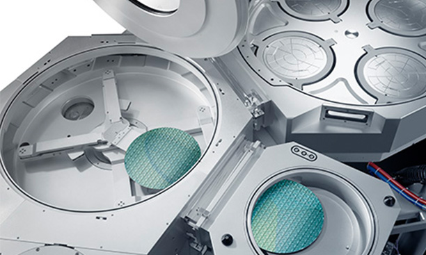
Deposition
Deposition processes create layers of dielectric (insulating) and metal (conducting) materials used to build a semiconductor device. Depending on the type of material and structure being made, different techniques are employed. Electrochemical deposition (ECD) creates the copper “wiring” (interconnect) that links devices in an integrated circuit. Metal plating of copper and other metals is also used for through-silicon vias and wafer-level packaging applications. Tiny tungsten connectors and thin barriers are made with the precision of chemical vapor deposition (CVD) and atomic layer deposition (ALD), which adds only a few layers of atoms at a time. Plasma-enhanced CVD (PECVD), high-density plasma CVD (HDP-CVD), and ALD are used to form the critical insulating layers that isolate and protect all of these electrical structures.
For the numerous materials and demanding features involved, our thin film deposition products provide the precision, performance, and flexibility needed for a wide range of challenging device applications.
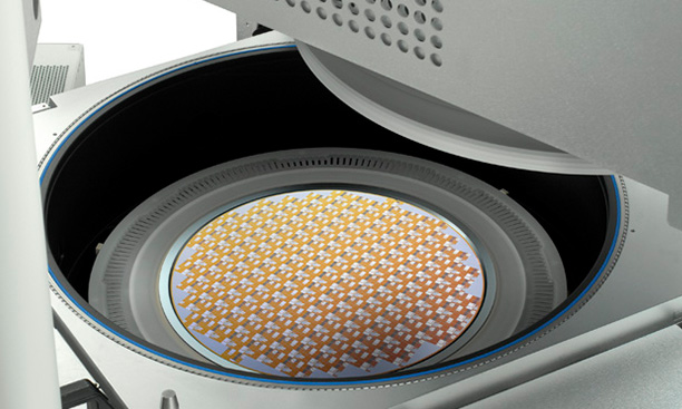
Etch
Etch processes help create chip features by selectively removing films and materials that have been deposited on the wafer. These processes involve fabricating increasingly small and complex features with complicated combinations of materials that need to be removed. The primary technology, reactive ion etch (RIE), activates the wafer surface with ions (charged particles) to remove material. Advanced etch techniques, such as atomic layer etching (ALE) are capable of removing a few atomic layers of material at a time. While conductor etch processes precisely shape electrically active components like transistors, dielectric etch forms the insulating structures that protect conducting parts. Etch processes also create the tall, high-aspect ratio features, such as through-silicon vias (TSVs), that allow packaging of chips together and for micro-electromechanical systems (MEMS).
Our plasma etch systems deliver the high-performance, high-productivity capabilities needed to form exacting structures – whether tall and narrow, short and wide, or measured in only a few angstroms.
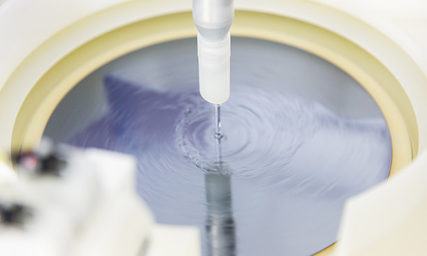
Strip & clean
Strip and clean techniques are used between manufacturing steps to eliminate unwanted material that could later lead to defects and to prepare the wafer surface for subsequent processing. Photoresist strip removes the photoresist film and residues following ion implant or etch steps. To clear away particles, contaminants, residues, and other unwanted materials, wafer cleaning steps are inserted throughout manufacturing. Wet processing technologies can be used for wafer cleaning as well as strip and etch applications. Plasma bevel cleaning is used to enhance die yield by removing unwanted materials from the wafer’s edge that could impact the device area.
Our strip technologies selectively remove remaining photoresist and provide process flexibility for multiple applications, while our high-productivity clean products deliver pristine surfaces center to edge for the most demanding cleaning steps.
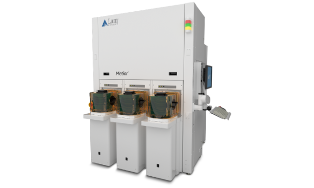
Mass metrology
Mass Metrology measures the change in mass following deposition, etch, and clean processes to enable monitoring and control of these often-repeated core manufacturing steps. This measurement enables Å-level quantification to process changes. Especially for processes involving high aspect-ratio structures, complex 3D architectures, OR Atomic Layer Deposition, optical techniques are limited in their ability to measure accurately the thick, deep, or otherwise visually obscured features. Measuring the change in mass for these applications provides a simple, accurate, high-precision yet high throughput solution for monitoring and control of the critical features in advanced device processes, where there is often little tolerance for variation.
Our line of high-precision mass metrology systems provides in-line monitoring and control of nearly all wafer-processing steps in real-time. Mass measurement is capable of recording minute changes on the wafer (incl. Queue time effect) in maximizing outlier detection while optimizing Metrology fleet investment.
The accuracy of mass change measurements has helped some critical processes to improve yield and device performance through inline and closed-loop feedback control. The breadth and depth of mass metrology have also enabled device manufacturers to improve chamber-matching and chamber-drift control. Such versatility has enabled many device manufacturers in maximizing the value of mass measurement to control the lifecycle of their wafers with Å-level precision and high throughput.