Leaving ultra-pristine surfaces
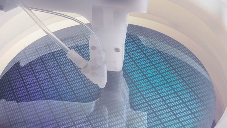
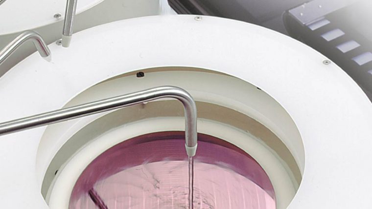
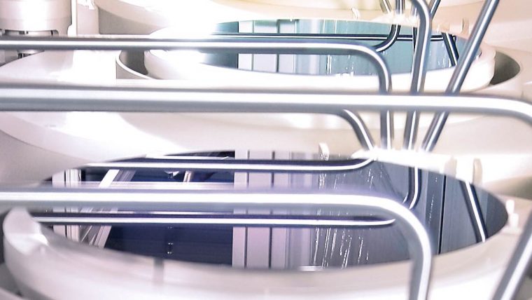
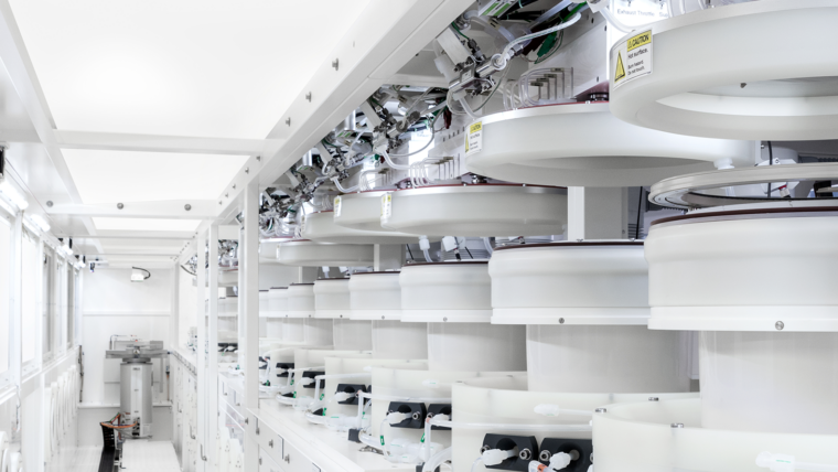
Strip and clean techniques are used between manufacturing steps to eliminate unwanted material that could later lead to defects and to prepare the wafer surface for subsequent processing. Photoresist strip removes the photoresist film and residues following ion implant or etch steps. To clear away particles, contaminants, residues, and other unwanted materials, wafer cleaning steps are inserted throughout manufacturing. Wet processing technologies can be used for wafer cleaning as well as strip and etch applications. Plasma bevel cleaning is used to enhance die yield by removing unwanted materials from the wafer’s edge that could impact the device area.
Lam’s strip technologies selectively remove remaining photoresist and provide process flexibility for multiple applications, while our high-productivity clean products deliver pristine surfaces center to edge for the most demanding cleaning steps.
Strip & Clean
OUR PRODUCTS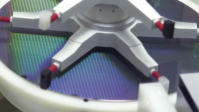
DV-Prime & Da Vinci Product Families
Wet Clean
These products provide the process flexibility needed with high productivity to address multiple wafer cleaning steps throughout manufacturing.
EOS Product Family
Wet Clean
Our advanced wet clean products deliver exceptionally low on-wafer defectivity at high throughput for progressively demanding applications.
Phoenix Product Family
Electrochemical Deposition (ECD) PR-Development PR-Strip Wet Clean/Strip
Phoenix offers a fully-automated high volume panel processing for 510x515mm substrates.
Reliant Clean Products
Reliant Systems Wet Clean/Strip
Our Reliant clean products enable roadmaps for Specialty Technologies and extend the productive life of fabs.
SP Series Product Family
Wet Clean
This proven product family delivers reliable, cost-efficient wet clean/wet etch solutions that gently remove unwanted materials from the wafer.
Triton Product Family
Electrochemical Deposition (ECD) Wet Clean/Strip
The Triton platform is a versatile and modular solution for single wafer plating and wet processing.
Related blog posts
-
Lam’s Collaborative Spare Parts Program Improves Chipmakers’ Cost Efficiency
Jun 27, 2023In the world of chipmaking, you may not necessarily think about the spare parts that a manufacturing tool uses as it builds the chip. Even more so than most factory machinery, chipmaking tools operate in extreme environments and create wear and tear on component parts, so spares are very much part of the equation. Lam Research’s spare parts programs help customers achieve their technology and cost goals by enabling tools to perform at the highest capability. One such program, Cost per Wafer Pass (CpWP), allows customers to better predict expenses, and improve manufacturing cost efficiency.
-
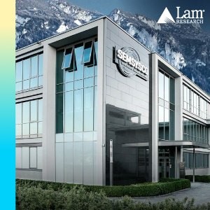
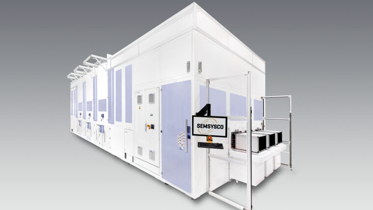
SEMSYSCO Joins Lam Research to Evolve the Advanced Packaging Substrate Market
Nov 15, 2022Today SEMSYSCO, a leading wet processing solutions company, announced that we have been acquired by Lam Research. We couldn’t be happier. At SEMSYSCO our mission is to overcome challenges through creative solutions and dynamic collaboration. We pride ourselves on offering innovative products and outstanding customer service. That sounds a lot like Lam Research, too. SEMSYSCO’s highly skilled and technical workforce has created a patented plating technology for large panels and a high-volume manufacturing platform for both panel cleans and panel plating.