Products
SP Series Product Family
Wet Clean
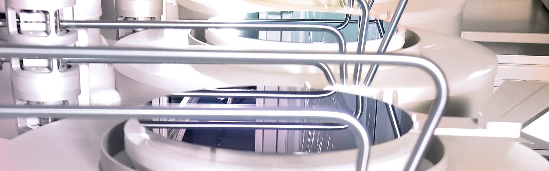
For advanced wafer-level packaging (WLP), the wet clean steps used between processes that form the package and external wiring have surprisingly complex requirements. These processes are called on to completely remove specific materials and leave other fragile structures undisturbed.
With a broad range of process capability, Lam’s SP Series products deliver cost-efficient, production-proven wet clean/wet etch solutions for these challenging WLP applications. For some applications, select models are also available through our Reliant® Systems as refurbished products, providing lower cost of ownership with the same quality assurance and performance as new systems.
Throughout the advanced wafer-level packaging (WLP) manufacturing sequence, wet processing steps are used for several key applications that vary widely in their process requirements. Wet clean processes must be capable of selectively and thoroughly removing residues from many surface types and feature shapes, including bonding pads, bumps, and high-aspect ratio (HAR) through-silicon vias (TSVs). Wet etch technologies are also used for WLP substrate thinning and wafer stress relief applications, which require fast-working, yet well-controlled processes. In addition, because of large feature sizes, high throughput and low-cost manufacturing are important.