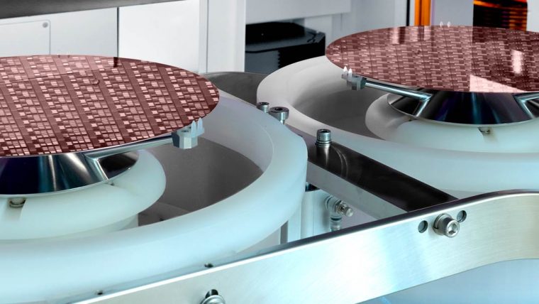
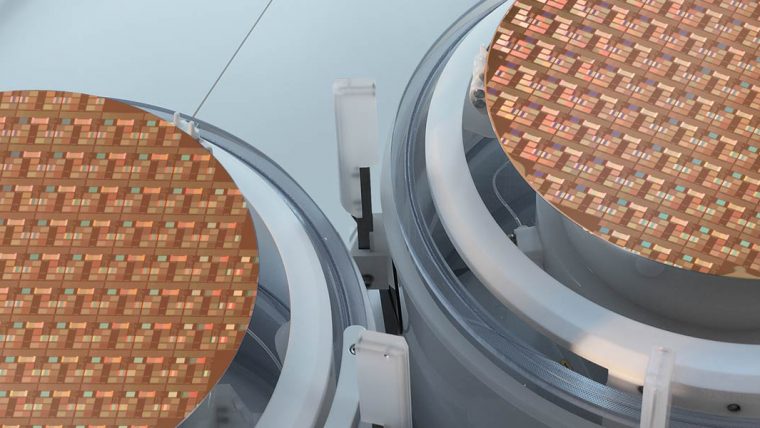
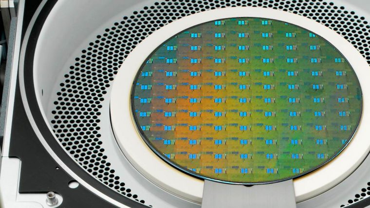
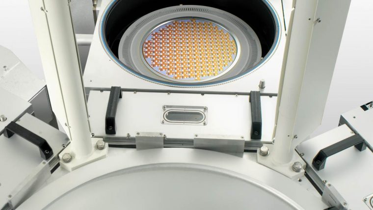
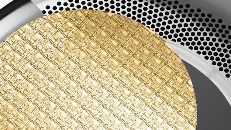
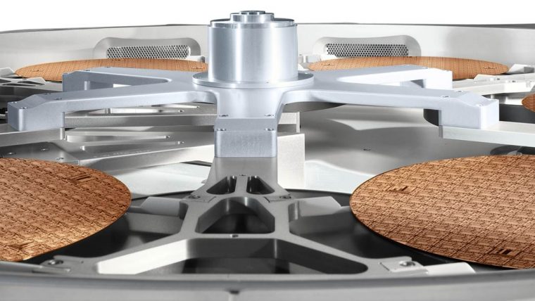
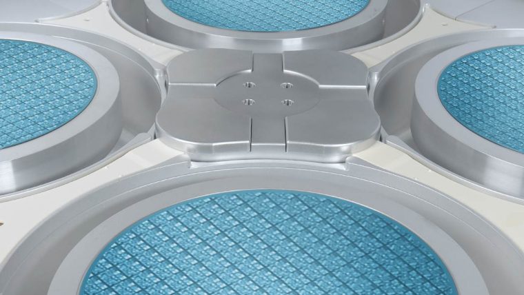
The future of technology is being shaped by the increasing prevalence of electronic devices, from smartphones and tablets to computers and gaming systems. The push for Artificial Intelligence (AI) is driving the need for more efficient and powerful processing hardware. Key advancements in semiconductor manufacturing focus on miniaturization, cost-performance ratios, and connectivity.
Advanced packaging technologies and chiplet designs are essential for meeting the demands of next-generation devices. Technologies such as wafer-level packaging (WLP), 3D through-silicon via (TSV) interconnects, and hybrid bonding are gaining traction, enabling heterogeneous integration and System-in-Package (SiP) solutions. The insatiable demand for computing power, driven by generative AI, is pushing the boundaries of package sizes, paving the way for large-format panel-level packaging and advanced glass substrates as the future of high-performance computing (HPC). These innovations allow multiple chips to be integrated into a single package, heralding a new era in device performance and design.
Packaging
Our SolutionsWETS Product Line
Delivering leading solutions in electroplating and wet processing including photoresist strip, etch and clean
SABRE 3D Product Family
Electrochemical Deposition (ECD)
Using our proven Electrofill technology, these high-productivity systems deliver quality metal films for advanced packaging applications.
SABRE Product Family
Electrochemical Deposition (ECD)
This product family offers precision metal plating for copper damascene manufacturing on the industry’s productivity-leading ECD platform.
SP Series Product Family
Wet Clean
This proven product family delivers reliable, cost-efficient wet clean/wet etch solutions that gently remove unwanted materials from the wafer.
DV-Prime & Da Vinci Product Families
Wet Clean
These products provide the process flexibility needed with high productivity to address multiple wafer cleaning steps throughout manufacturing.
Dry Etch Solutions
High-productivity solutions to overcome technically challenging requirements in advanced packaging, such as high-aspect -ratio etch (TSV, TDV & TGV) and Plasma Dicing
Syndion Product Family
Deep Reactive Ion Etch (DRIE) Reactive Ion Etch (RIE)
For deep etch applications, this product family provides the exceptional across-wafer uniformity control needed for critical high aspect ratio features.
Flex Product Family
Atomic Layer Etch (ALE) Cryogenic Etching Reactive Ion Etch (RIE)
Our dielectric etch systems offer application-focused capabilities for creating a wide range of challenging structures in advanced devices.
Kiyo Product Family
Reactive Ion Etch (RIE)
These market-leading conductor etch products deliver the high-performance precision and control at high productivity needed for critical device features.
GAMMA Product Family
Dry Strip
These products provide the process flexibility needed to address a wide range of critical photoresist strip applications.
Dielectric and Metal Deposition
Differentiated solutions for PECVD, ALD, and CVD metals. Enabling various film requirements for Advanced Packaging, including high-bond- strength dielectric, high quality inter-die gapfill film, and film stress tunability for wafer stress and shape management
VECTOR Product Family
Plasma-Enhanced Chemical Vapor Deposition (PECVD)
Our PECVD product family provides precise dielectric film deposition at high productivity for a wide range of device applications.
Striker Product Family
Atomic Layer Deposition (ALD)
Using advanced ALD technology, these products deliver dielectric films with exceptional control for critical processes in advanced devices with nanoscale features.
ALTUS Product Family
Atomic Layer Deposition (ALD) Chemical Vapor Deposition (CVD)
Combining CVD and ALD technologies, these market-leading systems deposit highly conformal metal films for advanced tungsten metallization applications.
Yield Improvement and Process Control
Innovative solutions to overcome challenges of emerging Advanced Packaging applications, such as wafer bevel management for wafer-to-wafer bonding yield improvement and high- throughput process control capability with mass metrology
Coronus Product Family
Plasma Bevel Etch and Deposition
Coronus systems focus on the bevel edge to enhance overall yield. Semiconductor processing can cause residues and roughness to accumulate along the wafer edge where they may flake off, drift to other areas, and create defects that cause a device to fail. Coronus etch products remove bevel residues and Coronus deposition protect the wafer bevel from damage.
Metior Product Family
Mass Metrology
Our mass metrology systems deliver sub-milligram measurement capability for advanced process monitoring and control of three-dimensional device structures.
Panel Processing Solutions
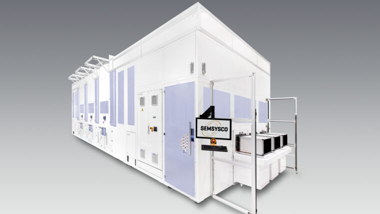
Transferring wafer-level processing technology, performance, and production yield, to panel-level processing. Delivering differentiated solutions for wet panel processing, such as Cu RDL, micro-bump, TGV and Cu build-up electroplating, PR/PI strip/develop, etch, roughening, and clean.
Kallisto Product Family
Electrochemical Deposition (ECD)
An advanced vertical processing platform for wet chemical treatment of substrates from 300x300mm up to Gen 5.1 (1100 x 1300mm) tailored to the needs of semi industry.
Phoenix Product Family
Electrochemical Deposition (ECD) PR-Development PR-Strip Wet Clean/Strip
Phoenix offers a fully-automated high volume panel processing for 510x515mm substrates.
Related Blog Posts
-
Advanced Semiconductor Packaging: The Secret Hero for the AI Infrastructure Era
June 24, 2024This report provides insight to the force and speed of innovation required to propel artificial intelligence (AI), new requirements from across the computing landscape, and why foundational principles of semiconductor manufacturing are requiring re-invention to deliver the performance and scale of this new age.
-

Advanced Packaging Furthers 3D Semi Structures and Extends Moore’s Law
May 20, 2024New developments in semiconductor packaging are contributing to the quest to extend Moore’s Law, the predictive model of adding more transistors to a semiconductor. One promising development is advanced packaging, which can better manage the power consumption of a collection of chips while shrinking their total size.
