
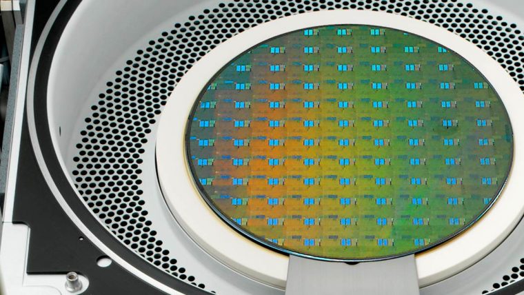
テクノロジーの未来は、スマートフォンやタブレット、コンピューター、ゲームシステムといった電子機器の普及拡大によって形作られつつあります。 人工知能(AI)の進展は、より高効率、より高性能な処理ハードウェアへの需要を加速させています。 半導体製造技術における主要な進歩は、微細化、コストパフォーマンス、そして接続性の向上に重点を置いています。
次世代デバイスの要求に応えるためには、先端パッケージング技術およびチップレット設計が不可欠となっています。 ウェハレベルパッケージング(WLP)や、3Dシリコン貫通ビア(TSV)インターコネクト、ハイブリッドボンディングなどの技術が注目を集めており、ヘテロジニアス・インテグレーションやシステム・イン・パッケージ(SiP)といったソリューションの実現を可能にしています。 生成AIによって牽引される計算能力への飽くなき需要は、パッケージサイズの限界を押し広げており、大判のパネルレベルパッケージングや先端ガラス基板といったハイパフォーマンス コンピューティング(HPC)の未来を支える新技術の台頭を後押ししています。 これらの革新により、複数のチップを単一のパッケージ内に統合することが可能となり、デバイスの性能と設計における新たな時代が到来しています。
パッケージング
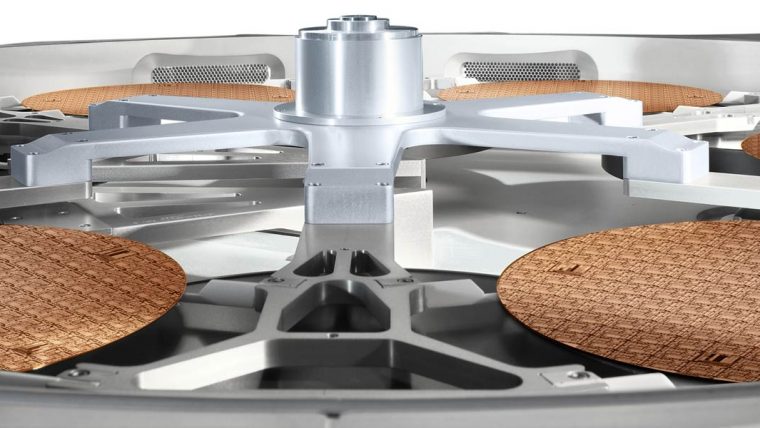
LamのソリューションWETS 製品ライン
電解メッキおよびウェットプロセス(フォトレジストの除去、エッチング、洗浄)における最先端のソリューションを提供
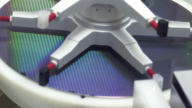
DV-PRIME & DA VINCI シリーズ
ウェットクリーニング
これらの製品は製造工程全体にわたる複数のウェハクリーニングステップにおいて求められる高い生産性と柔軟性を実現するプロセスを提供します。
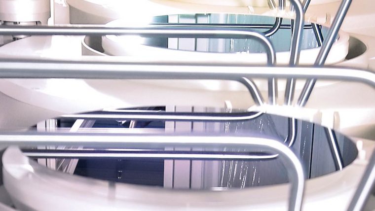
SP シリーズ製品
ウェットクリーニング
この実証済みの製品ファミリーは、ウェハから不要な材料を無理なく除去する、高信頼性、高コスト効率のウェットクリーニング/ウェットエッチングソリューションを提供します 。
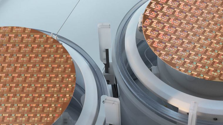
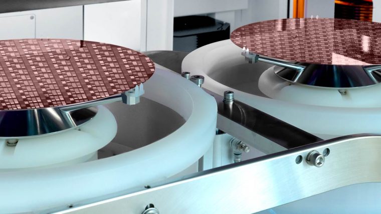
SABRE 3D シリーズ製品
電解メッキ (ECD)
一品および再生されたReliant製品は、コンダクター膜、酸化膜、および金属エッチング アプリケーションにおいて低所有コスト(低いランニングコスト)で、高信頼性、実証済みのソリューションを提供します。
ドライエッチングソリューション
高アスペクト比エッチング(TSV、TDV、TGV) やプラズマダイシングなどの先端パッケージングにおける技術的課題を克服する高生産性ソリューション

FLEX シリーズ製品
Atomic Layer Etch (ALE) クライオエッチング リアクティブ・イオンエッチング(RIE) 極低温エッチング
ラムリサーチの酸化膜エッチシステムは、先進のデバイスに求められる複雑な構造を備えた幅広いアプリケーションに配慮した機能を提供します。

KIYO シリーズ製品
リアクティブ・イオンエッチング(RIE)
業界をリードするコンダクターエッチング製品は、クリティカルなデバイス機能に必要な高精度と高い生産性での制御を実現します。
Syndion製品ファミリー
ディープリアクティブ・イオンエッチング(DRIE) リアクティブ・イオンエッチング(RIE)
ディープエッチング用途では、高アスペクト比の重要な形状に必要な卓越したウェーハ全体にわたる均一性制御を提供します。
絶縁膜および金属の成膜
PECVD、ALD、およびCVDメタル向けの差別化されたソリューション。 先端パッケージング向けのさまざまな成膜要件に対応:高接合強度の絶縁膜、高品質なダイ間ギャップフィル膜、ウェハ応力および形状管理のための膜応力制御性など
STRIKER シリーズ製品
原子層堆積(ALD)
高度なALD技術を活用することにより、これらの製品はナノスケールの機能を備えた高度なデバイスのクリティカルプロセスに対して優れた制御性能を実現する酸化膜を提供します。

VECTOR シリーズ製品
プラズマ化学気相成長(PECVD)
ラムリサーチ社のPECVD製品ファミリーは、幅広いデバイスアプリケーションに対応した高い生産性の精密な酸化膜成膜を提供します。
ALTUS製品ファミリー
化学気相成長(CVD) 原子層堆積(ALD)
CVDとALD技術を組み合わせた市場をリードするこれらのシステムにより、先進的なタングステンメタライゼーション用途向けに高コンフォーマルな金属膜を成膜します。
歩留まり向上とプロセス制御
新たな先端パッケージング技術における課題を克服する革新的ソリューション。例:ウェハ・トゥウェハ接合の歩留まり改善に向けたウェハベベル管理、質量計測による高スループットなプロセス管理など

CORONUSシリーズ製品
Plasma Bevel Etch and Deposition
半導体製造工程全体の歩留まりを向上させるためにCoronus システムはウェハのベベルエッジに着目しました。半導体製造工程を通じてウェハエッジ部には残渣や残膜 やラフネスが蓄積します。これが剥がれ落ちて他の場所に付着すると欠陥となり、デバイス不良を引き起こす原因なります。Coronus エッチはベベルの残渣を除去し、Coronus デポジションはベベルをダメージから保護する製品です。

METRYX シリーズ製品
Mass Metrology
ラムリサーチの質量計測システムは、高度なプロセス監視と3次元デバイス構造の制御により、サブミリグラムレベルの計測能力を提供します。
パネル加工ソリューション
ウェハレベルのプロセス技術・性能・歩留まりをパネルレベルプロセスへと移行・拡張。 Cu RDL、マイクロバンプ、TGV、Cuビルドアップ電解めっき、PR/PI剥離/現像、エッチング、粗化、洗浄など、ウェットパネルプロセス向けの差別化されたソリューションを提供します。
カリスト製品シリーズ
電解メッキ (ECD)
半導体業界のニーズに合わせた、300×300mmからGen5.1(1100x1300mm)までの基材をウェット処理するための先進的な縦型加工プラットフォーム。
フェニックス製品シリーズ
PR ストリップ PR 現像 ウェットクリーニング/ストリップ/エッチング 電解メッキ (ECD)
フェニックスは510x515mm 基板用の全自動大量パネル加工を提供します。