原子レベルの精度でパターンを加工
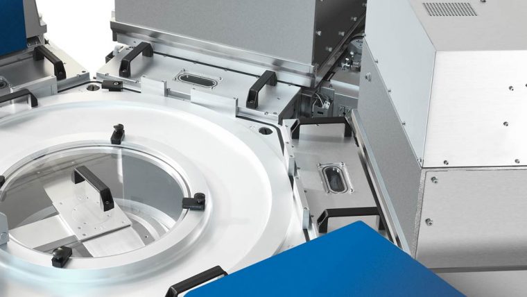
エッチング工程は、デポジション工程で形成した誘電体(絶縁膜)と金属(導電膜)を選択的に削り取って加工するプロセスです。このプロセスでは、加工対象となる材料が多くあるほか、その形状は微細化と複雑化を増す一方です。最も基本的な技法である反応性イオンエッチング(Reactive Ion Etching:RIE)はイオン(荷電粒子)をウェハ表面に叩き付けることで不要部分を削り取る技術です。加工形状が更に微細になると、原子層エッチング(ALE)が登場します。これは対象素材を原子数個分の厚さで少しずつ、繰り返し削って行くものです。メタルエッチングはトランジスタなどの電子素子の形を正確に加工するものですが、その一方で誘電膜エッチングは導体部分を保護する絶縁体を形成します。エッチングは、チップ間を接続するTSVやMEMSなどで使用される長い柱のような構造を加工するのにも利用されます。
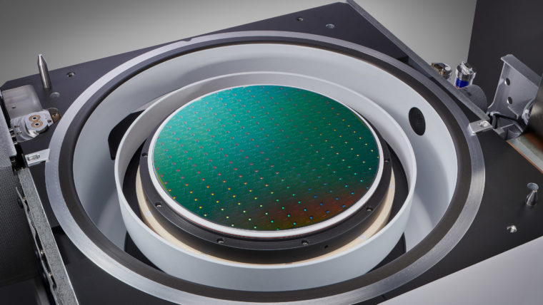
ラムリサーチのプラズマ・エッチング装置は、深く狭い・短く広いなど、わずか数nmの加工形状を正確に仕上げる高性能、高生産性を提供しています。
エッチング
当社の製品
CORONUSシリーズ製品
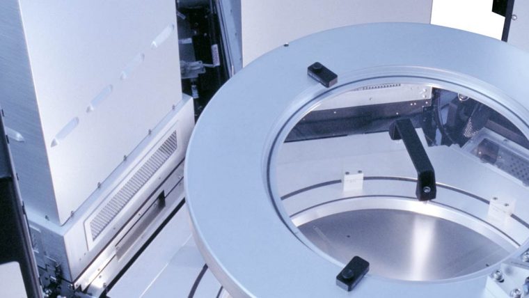
Plasma Bevel Etch and Deposition
半導体製造工程全体の歩留まりを向上させるためにCoronus システムはウェハのベベルエッジに着目しました。半導体製造工程を通じてウェハエッジ部には残渣や残膜 やラフネスが蓄積します。これが剥がれ落ちて他の場所に付着すると欠陥となり、デバイス不良を引き起こす原因なります。Coronus エッチはベベルの残渣を除去し、Coronus デポジションはベベルをダメージから保護する製品です。

FLEX シリーズ製品
Atomic Layer Etch (ALE) クライオエッチング リアクティブ・イオンエッチング(RIE) 極低温エッチング
ラムリサーチの酸化膜エッチシステムは、先進のデバイスに求められる複雑な構造を備えた幅広いアプリケーションに配慮した機能を提供します。

KIYO シリーズ製品
リアクティブ・イオンエッチング(RIE)
業界をリードするコンダクターエッチング製品は、クリティカルなデバイス機能に必要な高精度と高い生産性での制御を実現します。
RELIANTエッチング製品
RELIANT システム ディープリアクティブ・イオンエッチング(DRIE) リアクティブ・イオンエッチング(RIE)
当社の RELIANT エッチング製品は、スペシャルティ・テクノロジーのロードマップを実現し、ファブの生産寿命を延ばします。
SENSE.I製品
リアクティブ・イオンエッチング(RIE)
私たちの最新エッチング装置のプラットフォームは、最高の生産性でプロセスパフォーマンスを提供するコンパクトで高密度のアーキテクチャで比類のないシステムインテリジェンスを実現します。
Syndion製品ファミリー
ディープリアクティブ・イオンエッチング(DRIE) リアクティブ・イオンエッチング(RIE)
ディープエッチング用途では、高アスペクト比の重要な形状に必要な卓越したウェーハ全体にわたる均一性制御を提供します。
VANTEX シリーズ製品
クライオエッチング リアクティブ・イオンエッチング(RIE) 極低温エッチング
誘電体エッチングプロセスは、半導体デバイスの製造の中で非導電物質を除去します。特に業界最先端のメモリデバイスは、 ホールやトレンチの深さなどの難しい構造をもつため、厳しい公差で製造される必要があります。ラムリサーチの最新の誘電体エッチングシステムは、比類のない性能を実現し、厳しい高アスペクト比が求められるデバイスに生産性をもたらします。Vantex™は、進化したメモリデバイス製造の要件に対応する高度なRFテクノロジー、均一性制御およびEquipment Intelligence®を提供します。
VERSYS METAL シリーズ製品
リアクティブ・イオンエッチング(RIE)
これらのメタルエッチング製品は、電気配線およびメタルハードマスク用途向けに高い生産性を備えたプロセス制御を提供します。
Related Blog Posts
-

Etch Essentials: The Building Blocks of AI Era Microchips
Jun 12, 2024The artificial intelligence era depends on the storage infrastructure needed to run advanced technology, such as generative AI. The performance requirements for these AI innovations are pushing NAND devices to quickly scale to 400 vertically stacked layers and beyond. For readers who are new to semiconductors, that’s a big deal. Imagine a skyscraper with an unfathomable 400 floors, where each floor represents a layer of memory in a NAND device. Now, imagine adding 600 more floors to that building...only in semiconductors, this super tall structure is still invisible to the naked eye. Today, these devices range in height from a few micrometers (µm) to tens of micrometers.
-
How Etch Is Evolving to Meet the Demands of the AI Era
Nov 8, 2023The rise of artificial intelligence (AI) has placed significant demands on semiconductor performance, particularly in the realm of etching technology. AI requires massive amounts of data for training, necessitating high levels of parallel processing, non-volatile memory, and fast data transfer rates. To achieve these capabilities advanced devices are designed in three dimensions, leading to the need for novel etching techniques. Perpendicular etching, which involves removing materials in multiple directions, is essential for crafting gate-all-around (GAA) transistor architectures and precise modification of atomic layers. Aspect-ratio-dependent etching is crucial for the transition from 2D to 3D NAND architecture, enabling the efficient storage capacity increase by etching through numerous layers.