形成原子级精度的构件
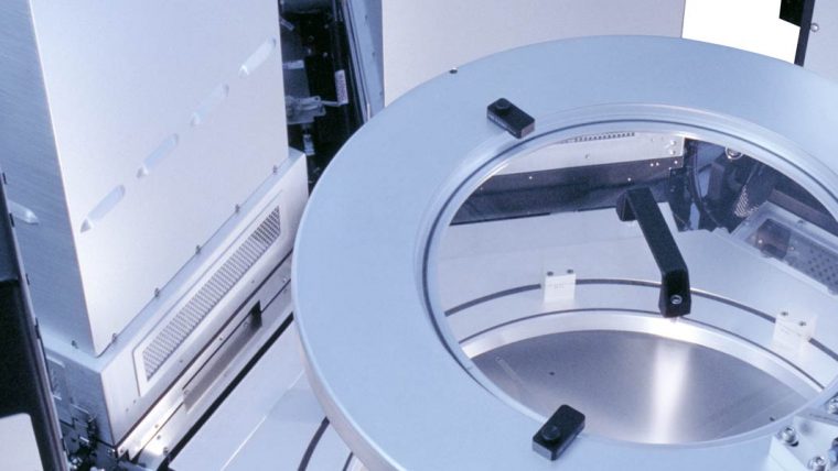
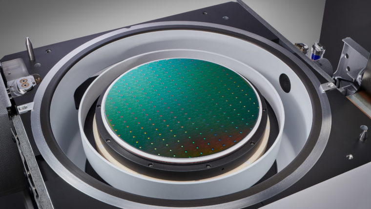
刻蚀工艺通过选择性地移除沉积过程中添加的介电(绝缘)材料和金属(导电)材料,协助形成芯片构件。这些工艺涉及使用多种材料制造越来越小、越来越复杂的高窄形构件。采用的主要技术为反应离子刻蚀(RIE),该技术用离子(带电粒子)轰击硅片表面,以移除相应的材料。对于最微小的构件,原子层刻蚀(ALE)可以一次移除数层原子层。导体刻蚀工艺精确地形成晶体管等重要电气组件,介电质刻蚀工艺则形成保护导电部分的绝缘结构。利用刻蚀工艺还可形成高柱状构件,如硅通孔(用于连接芯片)和微机电系统(MEMS)中所用构件。
无论高窄、短宽或是只有几纳米大小,泛林集团等离子刻蚀系统都可以为形成这些精确结构提供必要的高性能和高生产力。
刻蚀
我们的产品


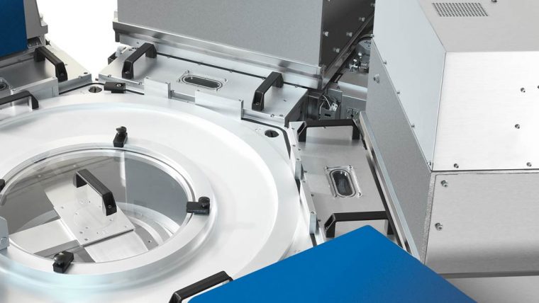
Vantex产品系列
低温刻蚀 反应离子刻蚀(RIE)
Vantex专为Sense.i平台设计,通过技术和Equipment Intelligence(设备智能)的创新,重新定义高深宽比刻蚀。
Related Blog Posts
-

Etch Essentials: The Building Blocks of AI Era Microchips
Jun 12, 2024The artificial intelligence era depends on the storage infrastructure needed to run advanced technology, such as generative AI. The performance requirements for these AI innovations are pushing NAND devices to quickly scale to 400 vertically stacked layers and beyond. For readers who are new to semiconductors, that’s a big deal. Imagine a skyscraper with an unfathomable 400 floors, where each floor represents a layer of memory in a NAND device. Now, imagine adding 600 more floors to that building...only in semiconductors, this super tall structure is still invisible to the naked eye. Today, these devices range in height from a few micrometers (µm) to tens of micrometers.
-
How Etch Is Evolving to Meet the Demands of the AI Era
Nov 8, 2023The rise of artificial intelligence (AI) has placed significant demands on semiconductor performance, particularly in the realm of etching technology. AI requires massive amounts of data for training, necessitating high levels of parallel processing, non-volatile memory, and fast data transfer rates. To achieve these capabilities advanced devices are designed in three dimensions, leading to the need for novel etching techniques. Perpendicular etching, which involves removing materials in multiple directions, is essential for crafting gate-all-around (GAA) transistor architectures and precise modification of atomic layers. Aspect-ratio-dependent etching is crucial for the transition from 2D to 3D NAND architecture, enabling the efficient storage capacity increase by etching through numerous layers.