
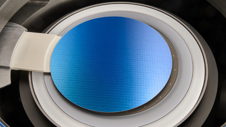
存储单元(存储电子数据的芯片元件)包括短期易失性(例如 DRAM)和长期非易失性(例如闪存)存储类型。 DRAM 是“工作”(主动)内存的支柱,而闪存则用于以紧凑的形式存储大量数据。
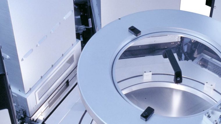
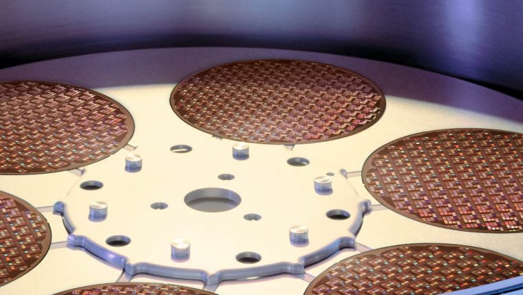
为了提高器件密度以获得更多存储容量,DRAM 特征不断缩小,NAND 闪存已转向三维架构,这带来了额外的工艺挑战。 例如,3D NAND 中的多层结构很容易受到应力的影响,高深宽比通道中的任何缺陷都可能造成电气短路和干扰。 由于使用了新型的、难以处理的材料,生产介于主动类和存储类之间的新型存储器也很困难。 因此,需要卓越的工艺控制、灵活性和生产率。

通过引领创新,泛林集团确保我们的存储解决方案满足不断变化的技术需求。 为了满足 AI、VR、AR 和电动汽车快速增长的需求,我们的高带宽内存(HBM)技术是我们正在创新的领域之一。 HBM 以其 3D 堆叠和尖端封装体现了高性能计算的未来,有望提供无与伦比的性能和效率。
面对先进存储器生产的复杂挑战,例如混合键合晶圆性能和良率管理,我们在微凸块和硅通孔(TSV)方面的专业知识使我们能够提供卓越的工艺控制和生产率。
高级内存
我们的解决方案


Fabtex™ Yield Optimizer
Semiconductor Yield Optimization Platform
Fabtex™ Yield Optimizer is a cutting-edge software platform designed to help semiconductor foundries accelerate yield ramp and improve high-volume manufacturing performance.


Vantex产品系列
低温刻蚀 反应离子刻蚀(RIE)
Vantex专为Sense.i平台设计,通过技术和Equipment Intelligence(设备智能)的创新,重新定义高深宽比刻蚀。

相关博客文章
-

The Road to the AI Era Is Paved in Semiconductor Manufacturing Innovation
Jun 24, 2024“The Road to the AI Era Is Paved in Semiconductor Manufacturing Innovation," an in-depth white paper written by The TechArena and sponsored by Lam Research, explores the pivotal role of chipmaking innovation in ushering in the next transformative technological age. The paper provides authoritative insights into the revolutionary effects of generative AI and large language models across various industries, the emerging challenges in delivering performance to meet these advanced requirements, and the critical importance of high bandwidth memory (HBM) in AI compute platforms.
-
Will HBM Redefine What's Possible With AI?
Mar 19, 2024There is a lot of buzz around high bandwidth memory (HBM). As artificial intelligence (AI) continues to advance so do its demands. Many major technology companies are betting on HBM to meet them. HBM is an advanced computer memory designed to offer faster data access with lower energy consumption. For AI, it can be a critical component in performance and reducing power consumption in memory chips.