
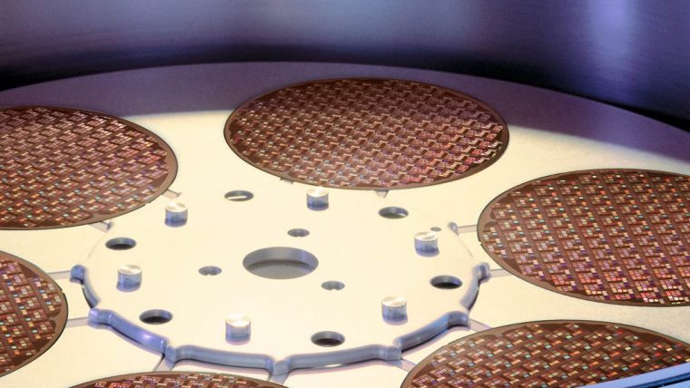
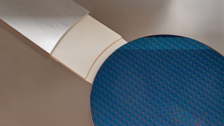
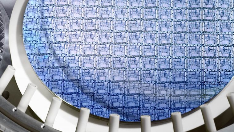
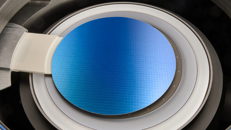
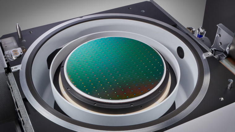
記憶體單元(儲存電子數據的晶片元件)包括短期揮發性(例如 DRAM)和長期非揮發性(例如快閃記憶體)儲存類型。 DRAM 是「工作」(活動)記憶體的支柱,而快閃記憶體則用於以緊湊的形式儲存大量數據。
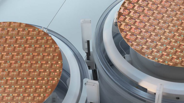
為了提高電子元件密度以獲得更多儲存容量,DRAM的結構特徵持續微縮,同時NAND 快閃記憶體已朝 3D 架構發展,這帶來了更多的製程挑戰。 例如,3D NAND 中的多層結構很容易受到應力的影響,高深寬比通道中的任何缺陷都可能造成電氣短路和干擾。 另一種介於活動型和儲存型記憶體之間的新型記憶體,因為採用了新穎、不易加工的材料,這類記憶體的生產也很困難。 因此,需要卓越的製程控制、靈活性和生產力。

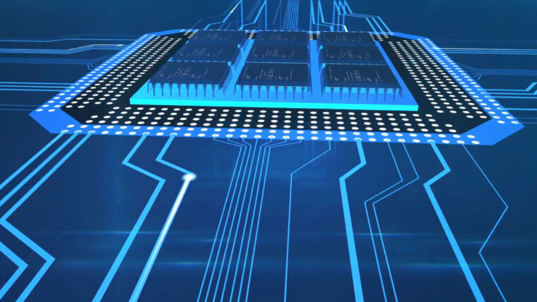
透過引領創新,科林研發確保我們的記憶體解決方案滿足不斷變化的技術需求。 為了滿足 AI、VR、AR 和電動汽車日益增長的需求,我們的高頻寬記憶體(HBM)技術是我們正在創新的領域之一。 HBM 以其 3D 堆疊和先進封裝展現了高效能運算的未來,可望提供無與倫比的效能和效率。
面對先進記憶體生產的複雜挑戰,例如混合接合晶圓效能和良率管理,我們在微凸塊和矽穿孔(TSV)方面的專業知識使我們能夠提供卓越的製程控制和生產力。
先進記憶體
我們的解決方案


Fabtex™ Yield Optimizer
Semiconductor Yield Optimization Platform
Fabtex™ Yield Optimizer is a cutting-edge software platform designed to help semiconductor foundries accelerate yield ramp and improve high-volume manufacturing performance.


相關部落格文章
-

The Road to the AI Era Is Paved in Semiconductor Manufacturing Innovation
Jun 24, 2024“The Road to the AI Era Is Paved in Semiconductor Manufacturing Innovation," an in-depth white paper written by The TechArena and sponsored by Lam Research, explores the pivotal role of chipmaking innovation in ushering in the next transformative technological age. The paper provides authoritative insights into the revolutionary effects of generative AI and large language models across various industries, the emerging challenges in delivering performance to meet these advanced requirements, and the critical importance of high bandwidth memory (HBM) in AI compute platforms.
-
Will HBM Redefine What's Possible With AI?
Mar 19, 2024There is a lot of buzz around high bandwidth memory (HBM). As artificial intelligence (AI) continues to advance so do its demands. Many major technology companies are betting on HBM to meet them. HBM is an advanced computer memory designed to offer faster data access with lower energy consumption. For AI, it can be a critical component in performance and reducing power consumption in memory chips.