製造無缺陷的
薄膜
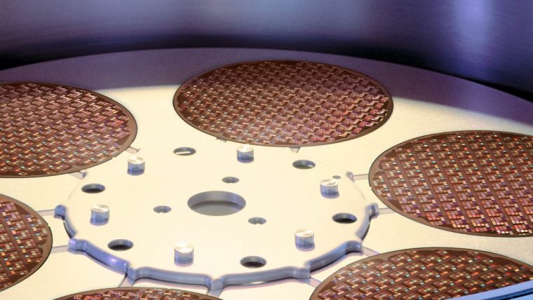
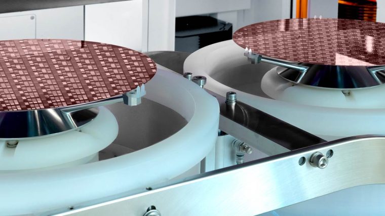
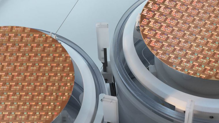
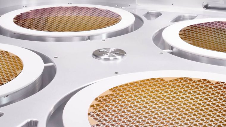
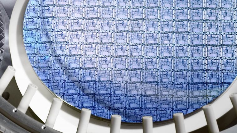
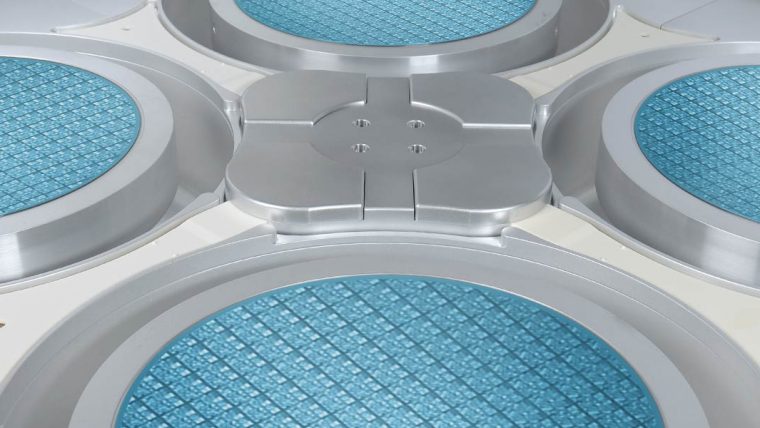
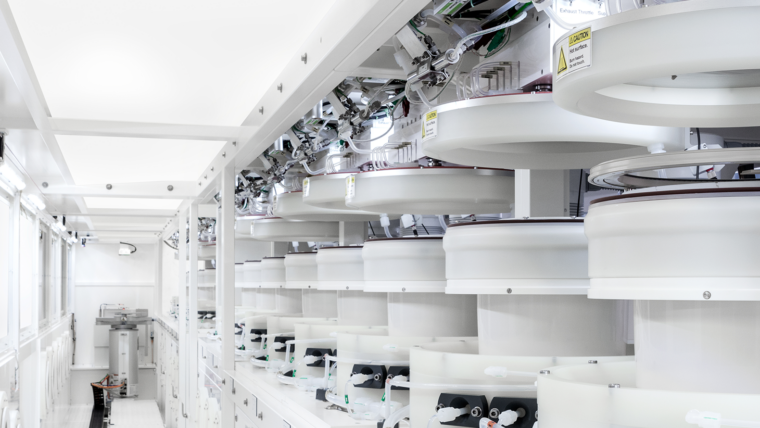
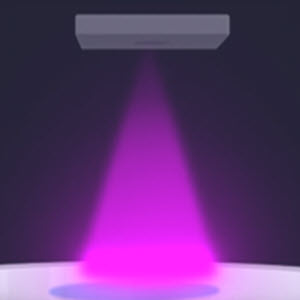
沉積製程可形成用於製造半導體元件的介電層(絕緣)和金屬(導電)材料層。 根據製作材料和結構的類型,會採用不同的技術。 電化學沉積(ECD)可生成連接積體電路中元件的銅「佈線」(互連)。 銅和其他金屬的金屬電鍍也用於矽穿孔和晶圓級封裝應用。 利用化學氣相沉積(CVD)和原子層沉積(ALD)技術,每次只需新增幾層原子,就能精確地製造出微小的鎢連接器和薄阻障層。 電漿輔助化學氣相沉積(PECVD)、高密度電漿化學氣相沉積(HDP-CVD)和原子層沉積(ALD)是用來形成隔離和保護所有這些電氣結構的關鍵絕緣層。使用脈衝雷射沉積(PLD)技術可實現高效能壓電層。PLD 是一種物理氣相沉積方法,它使用高脈衝能量雷射照射材料,產生沉積蒸氣,並將其凝結在不同的基板上。
對於所涉及的眾多材料和高要求特性,科林研發的薄膜沉積產品可為各種具有挑戰性的元件應用提供所需的精度、效能和廣泛應用性。
沉積
我們的產品

相關部落格文章
-
Lam’s Laser Focus on the Future of Chip Manufacturing
Mar 26, 2024Lam Research hopes to revolutionize microchip manufacturing with the launch of a new system: Prestis™. Why it matters: For the first time in semiconductor production, Lam is using lasers to deposit thin films and bringing pulsed laser deposition (PLD) to wafer-level mass production. Prestis is expected to be key in developing cutting-edge specialty technologies devices, such as RF (radio frequency) filters for 5G and Wi-Fi 6 and high-end MEMS (micro-electromechanical systems) microphones.
-
Introducing Coronus DX, World’s First Bevel Deposition Solution Optimized for 3D Chipmaking
Jun 20, 2023For more than 15 years, Lam’s Coronus® product family has been the leader in wafer bevel technology. Today we introduced the newest member of the family, Coronus DX. It’s the industry’s first bevel deposition solution optimized to tackle key manufacturing challenges in next-gen logic, 3D NAND and advanced packaging applications.