무결점
박막 형성
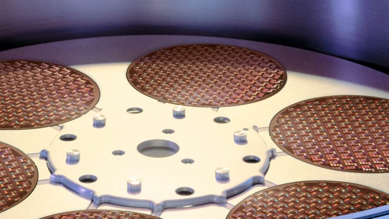
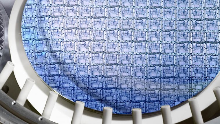
증착 공정은 반도체 소자를 만들 때 사용되는 유전(절연) 및 금속(전도) 재료 층을 형성하며, 재료의 유형과 형성되는 구조에 따라 다양한 기법이 사용됩니다. 전자기계 증착(ECD)에서는 소자를 집적 회로에 연결하는 구리 “배선”이 만들어집니다. 실리콘 관통 전극과 웨이퍼 수준의 패키징에는 구리와 기타 금속의 금속 도금도 사용됩니다. 작은 텅스텐 커넥터와 가는 보호막은 한 번에 단 몇 개의 원자층을 추가하는 정밀한 화학 증기 증착(CVD)과 원자층 증착(ALD)을 통해 만들어집니다. 플라스마 강화 CVD(PECVD), 고정밀 플라스마 CVD(HDP-CVD) 및 ALD는 이 모든 전기 구조물을 분리하고 보호하는 임계 절연층을 형성할 때 사용됩니다. 펄스 레이저 증착(PLD)은 고성능 압전층을 형성하는 데 사용됩니다. PLD는 고펄스 에너지 레이저로 물질에 에너지를 공급하여 증착 증기를 생성하는 물리적 증착 방법으로, 다양한 기판에 박막층을 증착합니다.
램리서치의 박막 증착 제품은 다양하고 까다로운 소자 부문에서 수많은 재료와 복잡한 피처를 다룰 때 필요한 뛰어난 정밀성, 성능, 유연성을 갖추고 있습니다.
증착
램리서치 제품
ALTUS 제품군
Chemical Vapor Deposition (CVD) 원자층 증착(ALD)
CVD 및 ALD 기술을 결합하여 시장을 선도하는 이 시스템은 고급 텅스텐 금속화 응용 분야를 위한 고도의 등각 금속 박막을 증착합니다.
Kallisto 제품군
Electrochemical Deposition (ECD)
300x300mm에서 1100x1100mm(5.1세대)까지 기판의 습식 화학 처리를 위한 첨단 수직 공정 플랫폼으로 반도체 업계의 요구 사항에 맞게 제작되었습니다.
Phoenix 제품군
Electrochemical Deposition (ECD) PR-Development PR-Strip Wet Clean/Strip/Etch
Phoenix는 510x510mm 기판의 완전 자동화된 대량 패널 처리를 제공합니다.
Prestis™
펄스 레이저 증착(PLD)
램리서치의 Prestis™ 제품군은 특수 기술 응용 분야의 다양한 복합 소재에 맞는 박막 증착 솔루션을 제공합니다.
Reliant Deposition 제품
Chemical Vapor Deposition (CVD) High-Density Plasma Chemical Vapor Deposition (HDP-CVD) Plasma-Enhanced Chemical Vapor Deposition (PECVD) Reliant Systems 펄스 레이저 증착(PLD)
램리서치의 Reliant 증착 제품군은 특수 기술의 로드맵을 지원하고 제조 시설의 생산 수명을 연장하는 솔루션을 제공합니다.
SABRE 3D 제품군
Electrochemical Deposition (ECD)
이 고생산성 시스템은 램리서치의 검증된 전기충진(Electrofill) 기술을 사용하여 첨단 패키징 분야에 필요한 양질의 금속막을 만듭니다.
SABRE 제품군
Electrochemical Deposition (ECD)
이 제품군은 업계 최고의 생산성을 자랑하는 ECD 플랫폼에서 구리 다마신을 제조할 때 필요한 고정밀 금속 도금 기능이 있습니다.
SOLA 제품군
Ultraviolet Thermal Processing (UVTP)
이 제품군은 박막의 특수 증착 후처리를 통해 첨단 박막 분야에 필요한 물리적 특성을 개선합니다.
SPEED 제품군
High-Density Plasma Chemical Vapor Deposition (HDP-CVD)
이 유전체 증착 제품은 업계 최고의 처리량과 신뢰성으로 고종횡비(high aspect ratio) 공간에 완벽한 갭필(gapfill)을 구현합니다.
Striker 제품군
원자층 증착(ALD)
첨단 ALD 기술을 사용하여 나노 수준의 피처가 있는 고급 소자의 주요 공정을 완벽하게 제어하는 유전막을 제공합니다.
Triton 제품군
Electrochemical Deposition (ECD) Wet Clean/Strip/Etch
Triton 플랫폼은 단일 웨이퍼 도금과 습식 처리를 위한 다목적 모듈 솔루션입니다.

VECTOR 제품군
Plasma-Enhanced Chemical Vapor Deposition (PECVD)
램리서치의 PECVD 제품군은 광범위한 소자 분야에서 높은 생산성으로 고정밀 유전막 증착을 실현합니다.
관련 블로그 기사
-
Lam’s Laser Focus on the Future of Chip Manufacturing
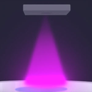
Mar 26, 2024Lam Research hopes to revolutionize microchip manufacturing with the launch of a new system: Prestis™. Why it matters: For the first time in semiconductor production, Lam is using lasers to deposit thin films and bringing pulsed laser deposition (PLD) to wafer-level mass production. Prestis is expected to be key in developing cutting-edge specialty technologies devices, such as RF (radio frequency) filters for 5G and Wi-Fi 6 and high-end MEMS (micro-electromechanical systems) microphones.
-
Introducing Coronus DX, World’s First Bevel Deposition Solution Optimized for 3D Chipmaking
Jun 20, 2023For more than 15 years, Lam’s Coronus® product family has been the leader in wafer bevel technology. Today we introduced the newest member of the family, Coronus DX. It’s the industry’s first bevel deposition solution optimized to tackle key manufacturing challenges in next-gen logic, 3D NAND and advanced packaging applications.