정밀 계측으로 공정 파악
질량 계측을 통해 증착, 식각, 세정 공정 후 질량의 변화를 측정하여 자주 반복되는 이러한 핵심 제조 단계를 모니터링하고 제어합니다. 박막 스택, 고종횡비 구조, 복잡한 3D 아키텍처 같은 디자인 구성요소의 경우, 광학 기법으로는 두껍거나, 깊거나, 불투명한 피처를 정확하게 측정하는데 한계가 있습니다. 이러한 용도에서 질량 변화를 측정할 수 있으면 변동 오차가 거의 없는 고급 소자 구조물의 임계 피처를 간단하고 정밀하게 모니터링하고 제어할 수 있습니다.
램리서치의 고정밀 질량 계측 시스템 라인은 증착, 식각, 세정 단계의 인라인 모니터링과 제어를 실시간으로 실행합니다. 미세한 질량 변화를 기록하여 잠재적 공정 변화를 정확하게 감지할 수 있습니다.
질량 계측
램리서치 제품
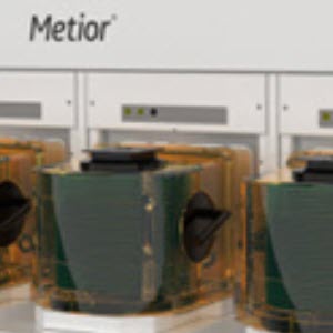
METRYX 제품군
Mass Metrology
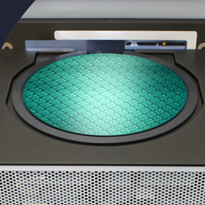
램리서치의 질량 계측 시스템에는 3차원 소자 구조의 첨단 공정 모니터링과 제어에 필요한 밀리그램 미만 단위의 측정 기능이 있습니다.
Related Blog Posts
-
Mass Metrology Applications Grow With Vertical Scaling
Jan 18, 2024In their ongoing effort to pack more computing power into less space, chip manufacturers are adopting scaling approaches that extend designs and stack components vertically—a major shift from the drive to shrink features horizontally that has dominated the industry for decades. This is especially true for memory devices like 3D NAND. To ensure the performance of these vertical designs, the dimensions of the thick film stacks and the high aspect ratio (tall and narrow) features must be tightly controlled, which requires precise measurement.
-
Metryx Marks 200th Tool Shipment With Classy Donation
Feb 2, 2023What is Metryx? Metryx develops and builds mass metrology tools for semiconductor manufacturers that monitor changes in a wafer’s mass as it goes through the wafer fabrication process. Why it matters: Metryx’s sensitive tools measure the weight of a silicon wafer before and after conducting some processes on the wafer, such as cutting pathways for the integrated circuit. The ability to accurately measure the weight change helps determine whether the operations were correctly completed, so the wafer can move to the next process step.