Products
SPEED Product Family
High-Density Plasma Chemical Vapor Deposition (HDP-CVD)
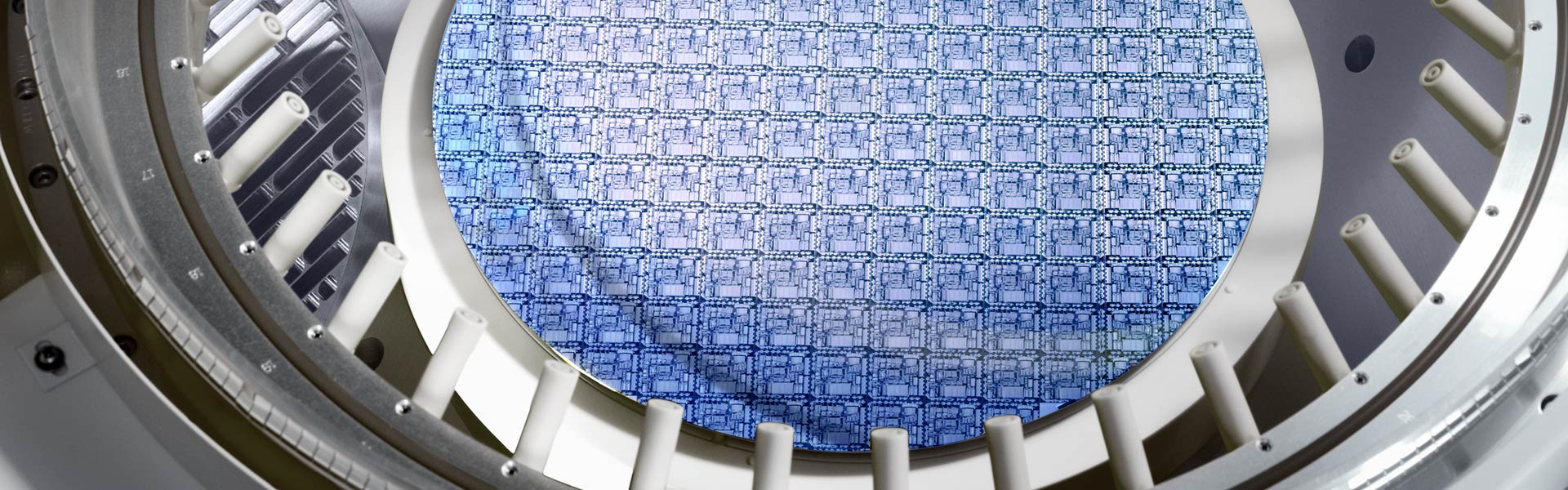
Dielectric “gapfill” processes deposit critical insulation layers between conductive and/or active areas by filling openings of various aspect ratios between conducting lines and between devices. With advanced devices, the structures being filled can be very tall and narrow. As a result, high-quality dielectric films are especially important due to the ever increasing possibility of cross-talk and device failure.
Lam’s SPEED® HDP-CVD products provide a multiple dielectric film solution for high-quality gapfill with industry-leading throughput and reliability. For some applications, select models are also available through our Reliant® Systems as refurbished products, providing lower cost of ownership with the same quality assurance and performance as new systems.
At advanced technology nodes, chipmakers continue to require high-quality dielectric films for gapfill processes to minimize integration complexity. Deposition processes that fill these advanced structures are challenged to achieve defect-free results while maintaining high throughput. For high aspect ratio (HAR) structures at advanced nodes, alternate gapfill technologies often do not deliver the film properties needed, resulting in poor process control and increased integration complexities. Preferred approaches are to use HDP-CVD either as a complete gapfill solution or as a cap over other gapfill technologies to enhance process control and mitigate integration risks.