
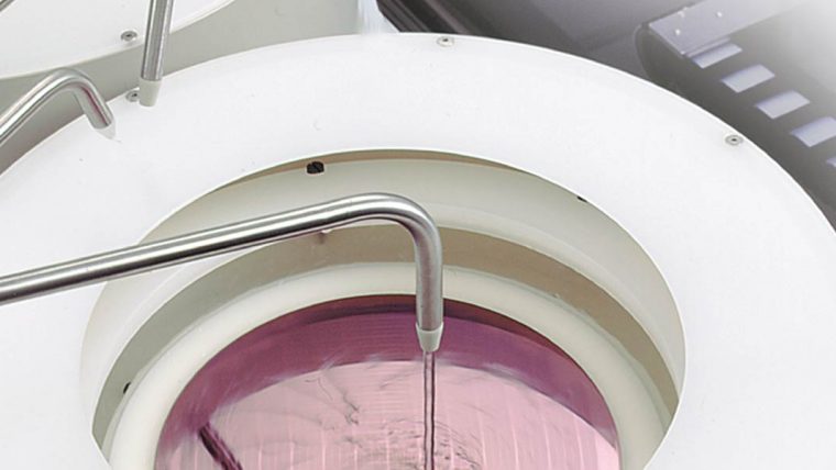
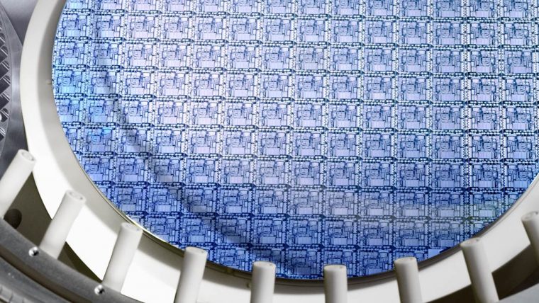
電晶體─亦即晶片的「大腦」─ 是控制電流流向的極小開關,在一顆晶片中可包含高達數十億個電晶體。隨著市場對更小,更強大電子產品的需求,推動了3D FinFET 等新型電晶體架構的發展,並使用高介電值(high-k)/金屬閘等特殊材料。這些新技術和新材料的發展使元件的特徵結構尺寸得以持續微縮。由於現今最新的電晶體尺寸已達到原子級,對製造而言是極大的挑戰。為確保這些先進元件的優異效能,製造功能需提供卓越的精密度與控制,才能形成所需的微小結構。
電晶體
解決方案


Fabtex™ Yield Optimizer
Semiconductor Yield Optimization Platform
Fabtex™ Yield Optimizer is a cutting-edge software platform designed to help semiconductor foundries accelerate yield ramp and improve high-volume manufacturing performance.


Related Blog Posts
-
Understanding CFETs, a Next Generation Transistor Architecture
Mar 21, 2024Computing power has experienced exponential growth over the last 70 years. This has largely been achieved through transistor scaling. Due to a continuous reduction in the size of transistors, engineers have been able to pack more and more of them onto a single chip[1]. This has led to faster, more powerful, and more energy-efficient devices. Improvements in fabrication processes and materials, along with better circuit design techniques, have enabled this scaling. As transistors have become smaller and more densely packed, we have started to reach limitations caused by the laws of physics.
-
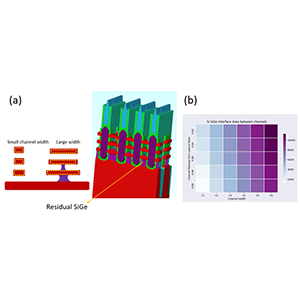
Improving Gate All Around (GAA) Transistor Performance using Virtual Process Window Exploration
Jun 14, 2023As transistor sizes shrink, short channel effects make it more difficult for transistor gates to turn a transistor ON and OFF [1]. One method to overcome this problem is to move away from planar transistor architectures toward 3D devices. Gate-all-around (GAA) architectures are an example of this type of 3D device [2]. In a GAA transistor, the gate oxide surrounds the channel in all directions. A key process during the fabrication of GAA transistors involves the channel release step.