Lam is leading the way in next generation DRAM
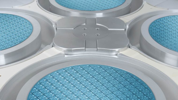
The continued growth in PCs, laptops, mobile phones, and data centers has propelled DRAM into its sixth generation of 10-nm-class chips, known as 1-gamma. To keep pace with power, speed and density requirements, DRAM manufacturers are expected to continue extending the planar roadmap by transitioning cell architecture from 6F² to 4F², pushing well into sub-10nm territory by 2028.
With decades of proven expertise and technical leadership, Lam is enabling customers to advance planar DRAM technologies to sub-10nm nodes.
AI is driving the need for
high-performance DRAM
Artificial intelligence accelerators can execute massive amounts of math in parallel, but they only run at full speed when data arrives just as quickly. DRAM serves as the working memory that feeds the data to these chips.
As models get larger and prompts get longer, systems need:
- Higher bandwidth to keep accelerators busy
- More capacity to hold parameters and activations
- Lower latency for quicker responses
- Better energy efficiency to control power and operating costs
The result is that modern AI workloads have grown increasingly memory-bound. Meeting these demands will require advanced DRAM supported by best-in-class process technologies to unlock full performance.
Meeting increased memory demands
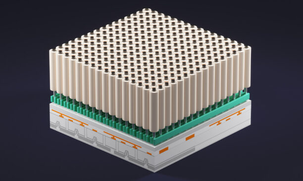
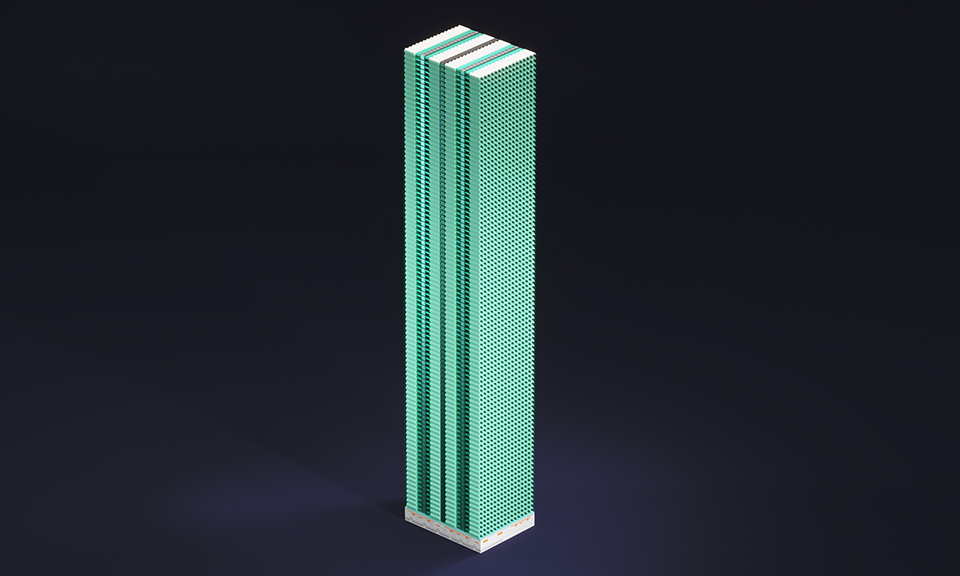
Supporting these rapidly evolving workloads will require denser, more complex architectures and new integration approaches. Industry shifts—such as tighter cell layouts and CMOS‑to‑memory wafer bonding that more than doubles metal wiring levels—sharpen requirements for precision patterning, etch and void‑free conformal fill with exceptional depth uniformity and profile control.
DRAM customers demand tighter specs, higher uniformity, and proven performance. These are exactly the pressure points Lam’s portfolio targets (Akara® etch, Aether® dry resist, ALTUS® Halo molybdenum fill, Striker® ALD), and why we are positioned to enable continued 2D scaling and support customer roadmaps for the 3D DRAM transition.
How Lam Research is enabling continued evolution
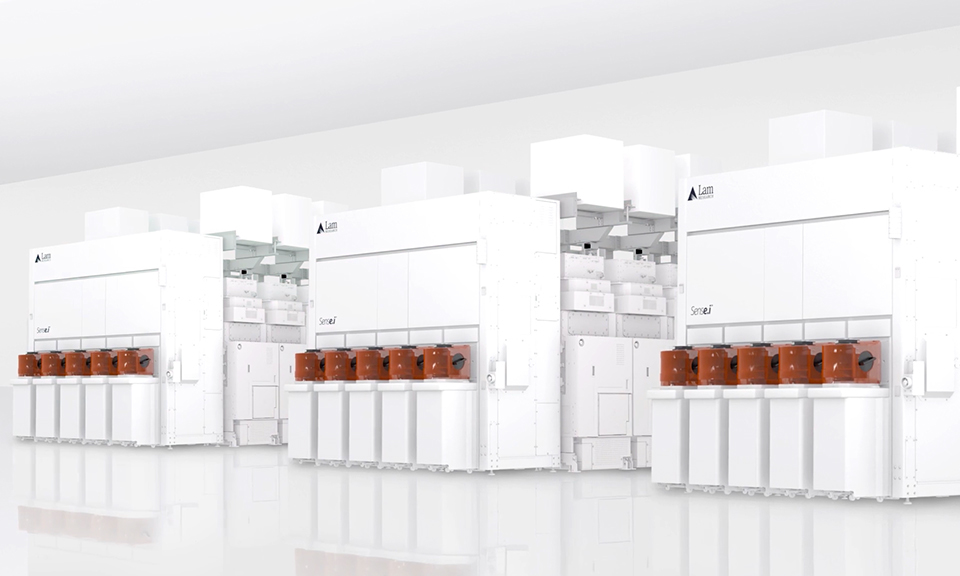
Building on our success in NAND while recognizing DRAM’s unique challenges, Lam is providing the critical process technologies that make next generation DRAM possible. Our differentiated portfolio—Akara, Aether, Halo, Striker—delivers precision, uniformity, and integration excellence to meet the most demanding specs in memory manufacturing.
We are also actively investing in the future of DRAM through:
- Strategic collaborations with imec, universities (TIE at University of Texas, NCTU Taiwan), and Resonac.
- Continuous innovation in materials science and process technology to address future inflections.
- Lam Capital investments in emerging businesses that complement our portfolio.
Our Solutions
Lam’s DRAM solutions address critical challenges in patterning, etch, and deposition, enabling customers to extend 2D DRAM and prepare for 3D architectures with confidence.
Our strategic focus areas for DRAM include:
- (Planar DRAM) Sub-10nm patterning using EUV (Aether)
- (Planar DRAM) Sub-10nm Si etching to form transistors (Kiyo® → Akara)
- (Planar DRAM) bending-free gapfill (Striker), low-k spacer (Striker SPARC)
- (3D DRAM) – ultra high A/R etching for Si/SiGe (Akara)
- (3D DRAM) – ultra high A/R oxide gapfill (Striker, Halo)
- (HBM) – TEOS® 3D, SABRE®, Syndion® etcher
- Backside deposition for shape control and integration
- Process uniformity across high-aspect-ratio structures