원자 수준의 정밀도로 피처 형성
식각 공정에서는 증착 시에 첨가된 유전(절연) 및 금속(전도) 물질을 선택적으로 제거하여 칩 피처의 형성을 돕습니다. 이러한 공정에서는 여러 종류의 재료를 사용하여 더 작고, 복잡하고, 길고 가는 피처를 제작해야 합니다. 1차 기술인 반응성 이온 식각(RIE)을 통해 웨이퍼 표면에 이온(하전 입자) 충격을 가하여 물질을 제거합니다. 가장 작은 피처의 경우는 원자층 식각(ALE)을 통해 한 번에 몇 개의 원자층을 제거합니다. 전도체 식각 공정은 트랜지스터 같은 임계 전기 구성요소의 형상을 정밀하게 만들고, 유전체 식각은 전도성 부품을 보호하는 절연 구조물을 형성합니다. 식각 공정에서는 칩을 서로 연결하는 TSV와 미세전자기계시스템(MEMS)에서 사용되는 기둥 모양의 기다란 피처도 만듭니다.
램리서치 제품
식각

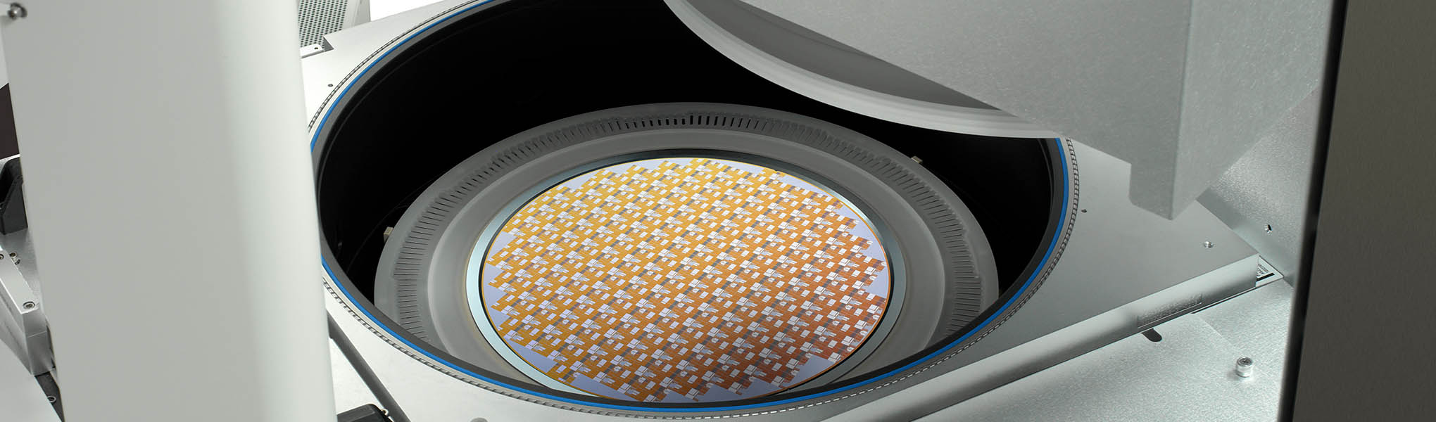
Akara®
Akara®는 밀리초 단위로 단축한 공정 반응 시간을 통해 웨이퍼 출력을 증가시키고, 낭비되는 시간을 줄여 최대의 공정 수율을 제공합니다. 업계에서 가장 앞선 식각 균일성 제어 기술로 옹스트롬 수준의 높은 균일성과 웨이퍼 간 반복성을 제공합니다.

CORONUS 제품군
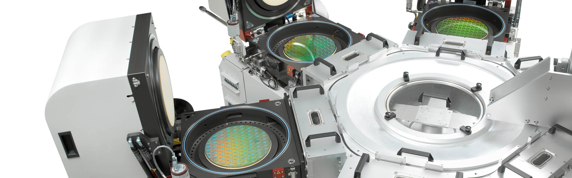
Coronus 시스템은 웨이퍼 베벨 엣지에 중점을 두어 전반적인 수율을 높입니다. 반도체 공정 진행 시 웨이퍼 가장자리를 따라 잔여물과 거칠기가 누적됩니다. 이는 웨이퍼의 다른 영역으로 떨어져 날리면 장치의 고장을 유발하는 결함을 발생시킬 수 있습니다. Coronus 식각 제품은 웨이퍼 베벨에 있는 잔여물을 제거하고 Coronus 증착 제품은 웨이퍼 베벨이 손상되지 않도록 보호합니다.
FLEX 제품군
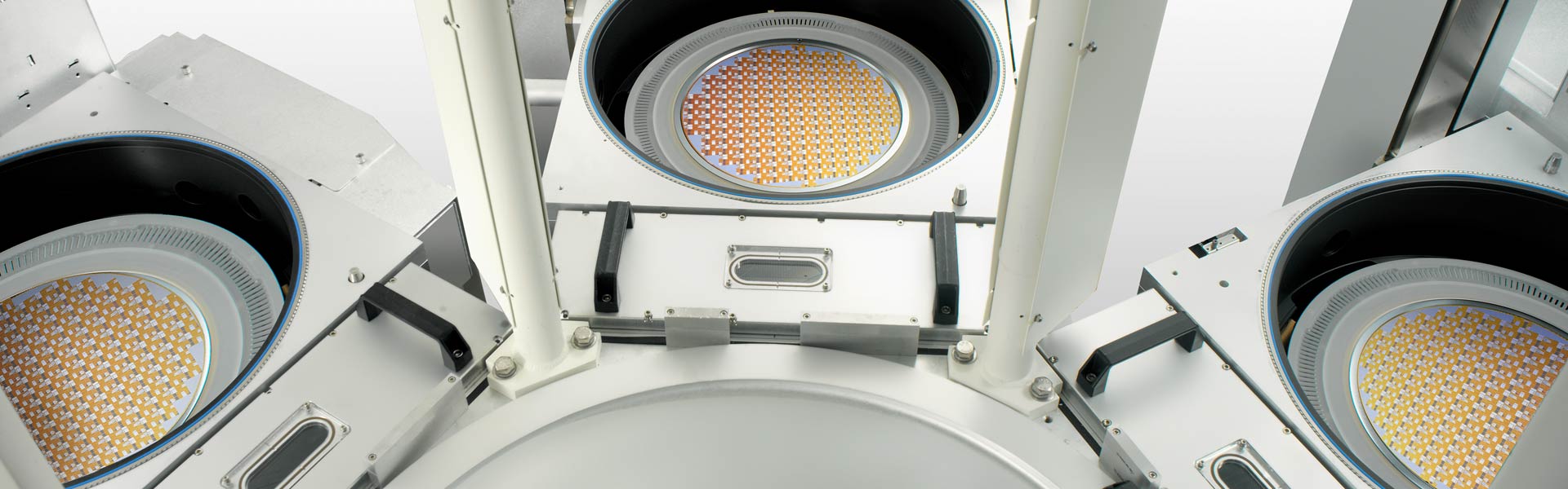
램리서치의 유전체 식각 시스템은 용도에 맞춘 기능 덕분에 고급 소자의 까다로운 구조를 다양하게 만들 수 있습니다.
KIYO 제품군
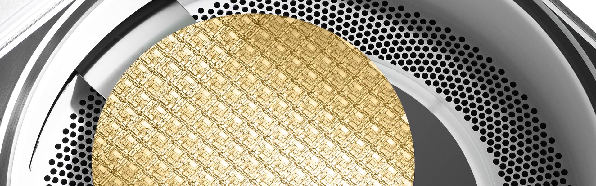
시장을 선도하는 램리서치의 전도체 식각 제품은 주요 소자 피처(feature)에 요구되는 고성능 정밀도와 제어력이 특징입니다.
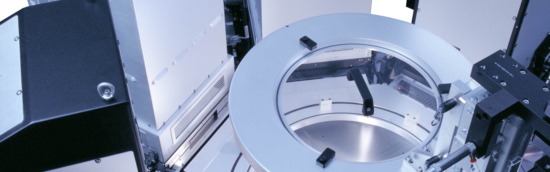
Reliant Etch 제품
램리서치의 Reliant 식각 제품군은 특수 기술의 로드맵을 지원하고 제조 시설의 생산 수명을 연장하는 솔루션을 제공합니다.
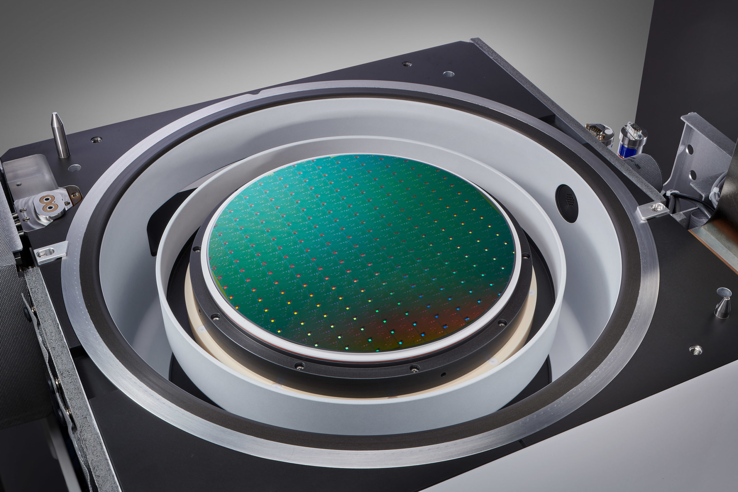
고선택비 식각 제품군
획기적인 고선택비 식각 장비 포트폴리오는 3D 구조와 첨단 로직 및 파운드리 애플리케이션을 위한 옹스트롬(Å) 수준의 정밀도와 초고도 선택비 기반의 역량으로 등방성 식각을 지원합니다.
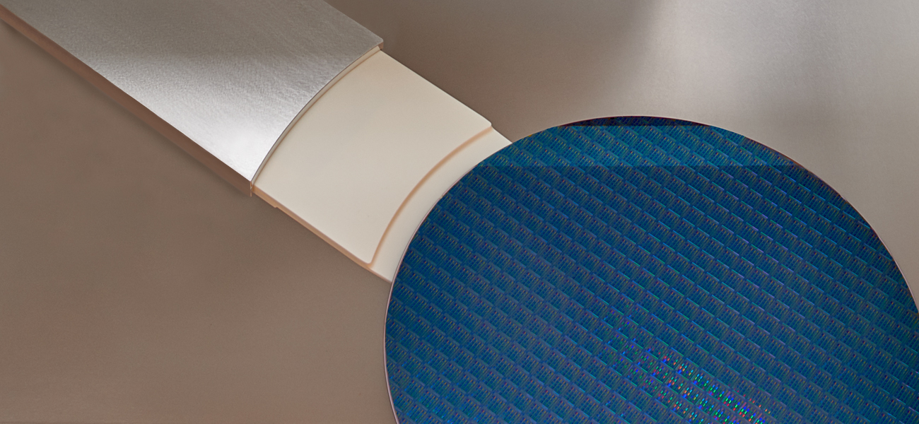
SENSE.I 제품군
램리서치의 최신 식각 플랫폼은 컴팩트한 고밀도 구조에 누구도 따라올 수 없는 시스템 지능을 갖추고 있어 공정 성능을 최고의 생산성으로 구현합니다.
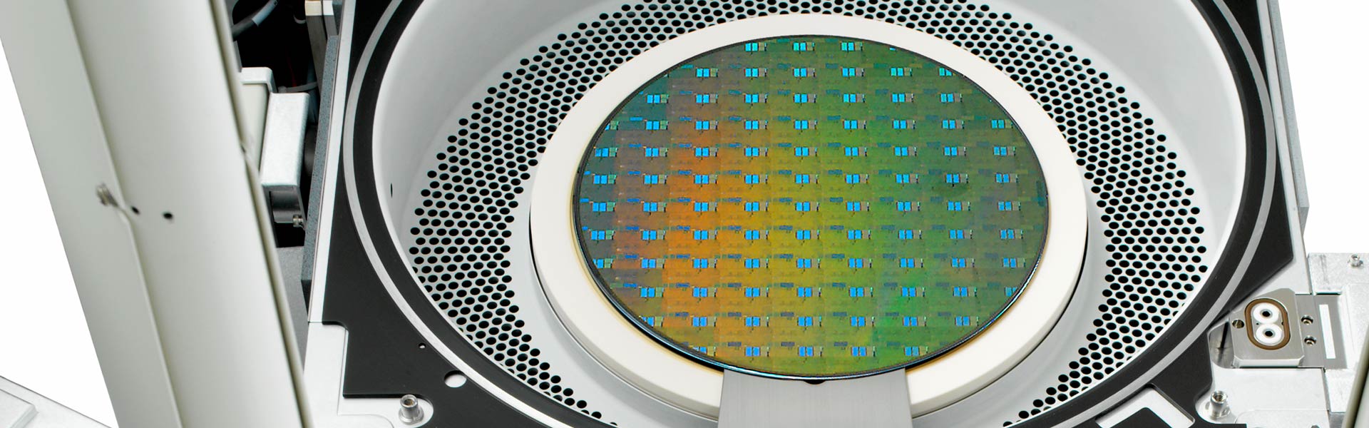
Syndion 제품군
딥 식각 응용 부문에서 이 제품군은 고종횡비 피처를 형성하는 데 필요한 우수한 웨이퍼 균일도 제어 능력을 제공합니다.
VANTEX 제품군
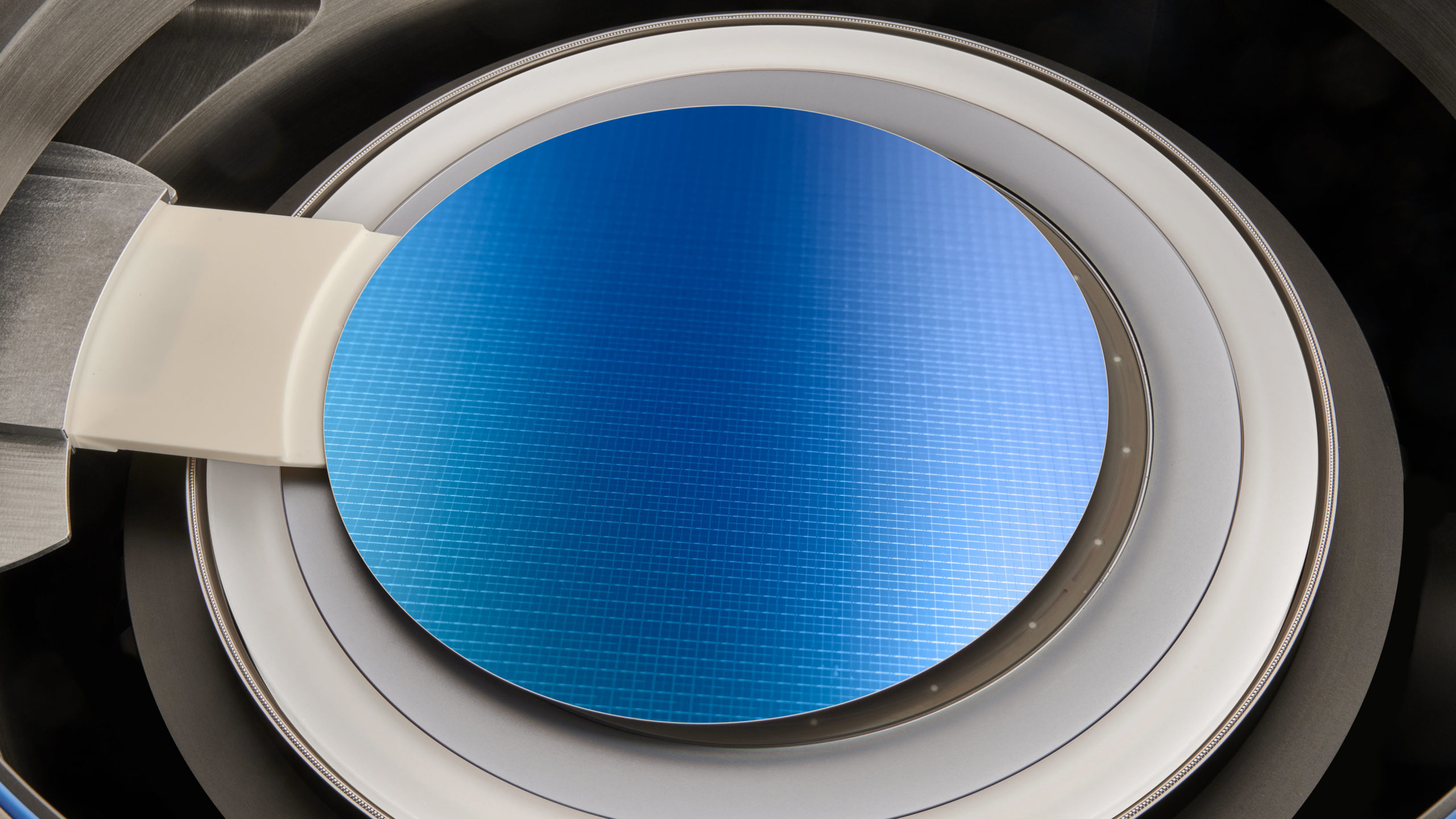
Sense.i 플랫폼용으로 설계한 Vantex는 기술 혁신과 Equipment Intelligence로 고종횡비 식각을 새롭게 정의합니다.
VERSYS METAL 제품군
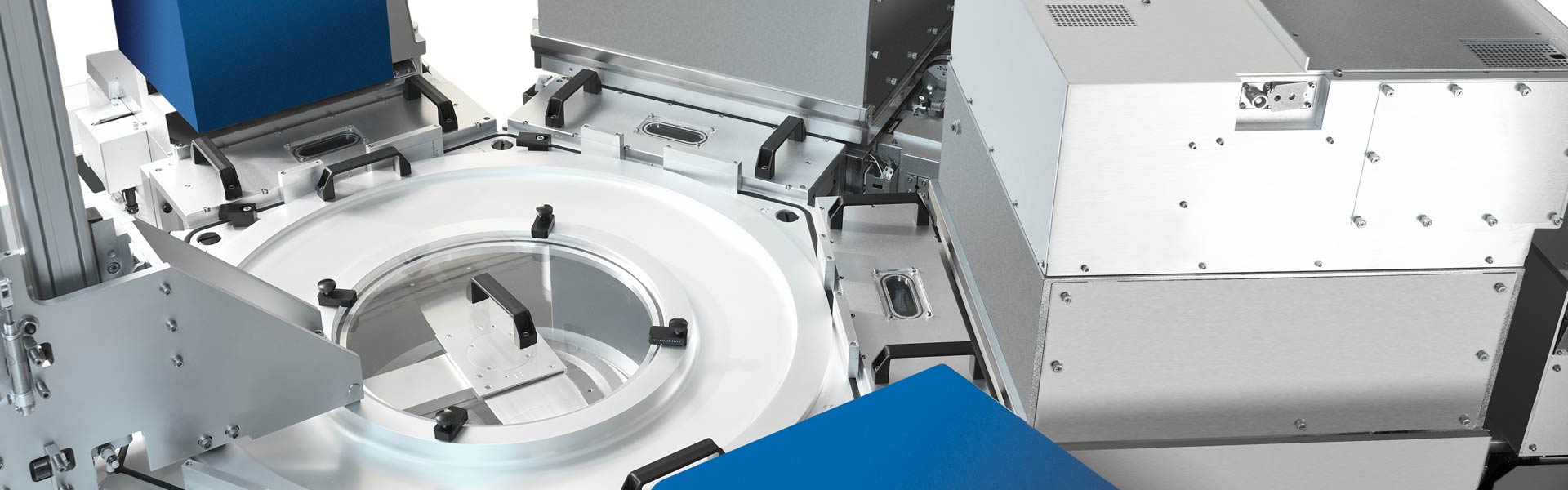
이 금속 식각 제품은 전기 연결 및 금속 하드마스크 분야에서 높은 생산성으로 공정을 완벽하게 제어합니다.
Related blog posts
Etch Essentials: The Building Blocks of AI Era Microchips
The artificial intelligence era depends on the storage infrastructure needed to run advanced technology, such as generative AI. The performance requirements for these AI innovations are pushing NAND devices to quickly scale to 400 vertically stacked layers and beyond. For readers who are new to semiconductors, that’s a big deal. Imagine a skyscraper with an unfathomable 400 floors, where each floor represents a layer of memory in a NAND device. Now, imagine adding 600 more floors to that building...only in semiconductors, this super tall structure is still invisible to the naked eye. Today, these devices range in height from a few micrometers (µm) to tens of micrometers.
How Etch Is Evolving to Meet the Demands of the AI Era
The rise of artificial intelligence (AI) has placed significant demands on semiconductor performance, particularly in the realm of etching technology. AI requires massive amounts of data for training, necessitating high levels of parallel processing, non-volatile memory, and fast data transfer rates. To achieve these capabilities advanced devices are designed in three dimensions, leading to the need for novel etching techniques. Perpendicular etching, which involves removing materials in multiple directions, is essential for crafting gate-all-around (GAA) transistor architectures and precise modification of atomic layers. Aspect-ratio-dependent etching is crucial for the transition from 2D to 3D NAND architecture, enabling the efficient storage capacity increase by etching through numerous layers.