
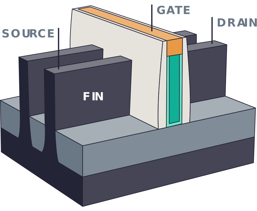
칩의 “두뇌”인 트랜지스터는 전기의 흐름을 제어하는 작은 스위치로, 단일 집적 회로 안에 수십 억 개가 들어갈 수 있습니다.더 작고, 더 강력한 전자장치에 대한 요구 때문에 3D FinFET 디자인 같은 새로운 트랜지스터 아키텍처가 개발되고, 고유전/금속 게이트 같은 특수 재료가 사용되고 있습니다. 이 덕분에 소자 피처의 크기는 계속 작아지고 있습니다.현재 최신 트랜지스터는 치수가 원자 수준이기 때문에 제조하기가 매우 어렵습니다.이러한 고급 소자에 요구되는 높은 성능을 실현시키기 위해서는 작은 피처를 매우 정밀하게 제어해 가며 만들 수 있는 제조 능력이 필요합니다.
램리서치 솔루션
트랜지스터
ALTUS 제품군
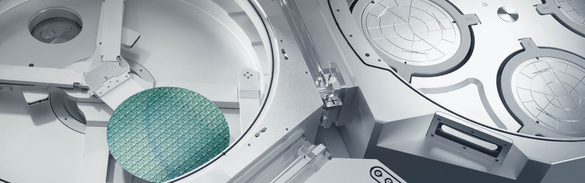
CVD 및 ALD 기술을 결합하여 시장을 선도하는 이 시스템은 고급 텅스텐 금속화 응용 분야를 위한 고도의 등각 금속 박막을 증착합니다.

CORONUS 제품군
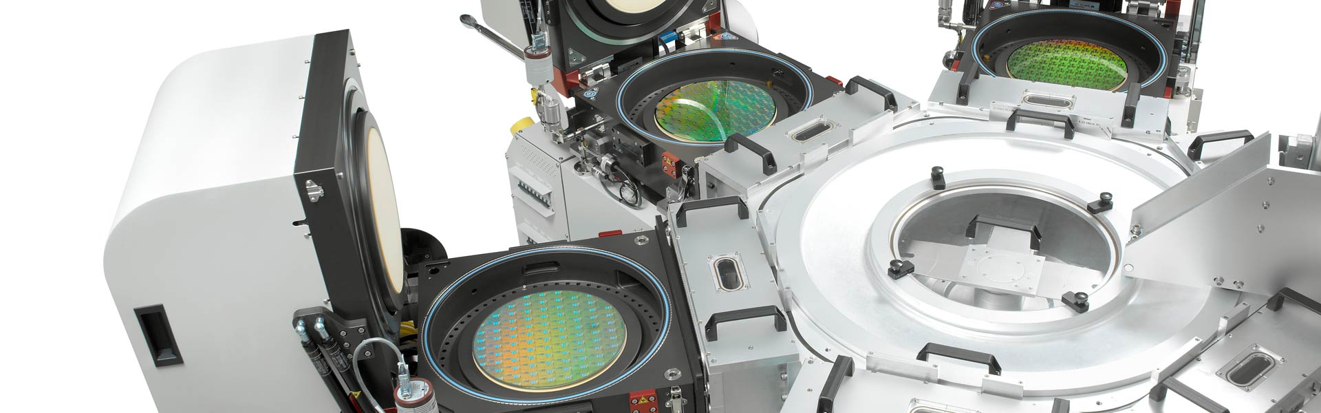
Coronus 시스템은 웨이퍼 베벨 엣지에 중점을 두어 전반적인 수율을 높입니다. 반도체 공정 진행 시 웨이퍼 가장자리를 따라 잔여물과 거칠기가 누적됩니다. 이는 웨이퍼의 다른 영역으로 떨어져 날리면 장치의 고장을 유발하는 결함을 발생시킬 수 있습니다. Coronus 식각 제품은 웨이퍼 베벨에 있는 잔여물을 제거하고 Coronus 증착 제품은 웨이퍼 베벨이 손상되지 않도록 보호합니다.
DV-Prime & Da Vinci 제품군
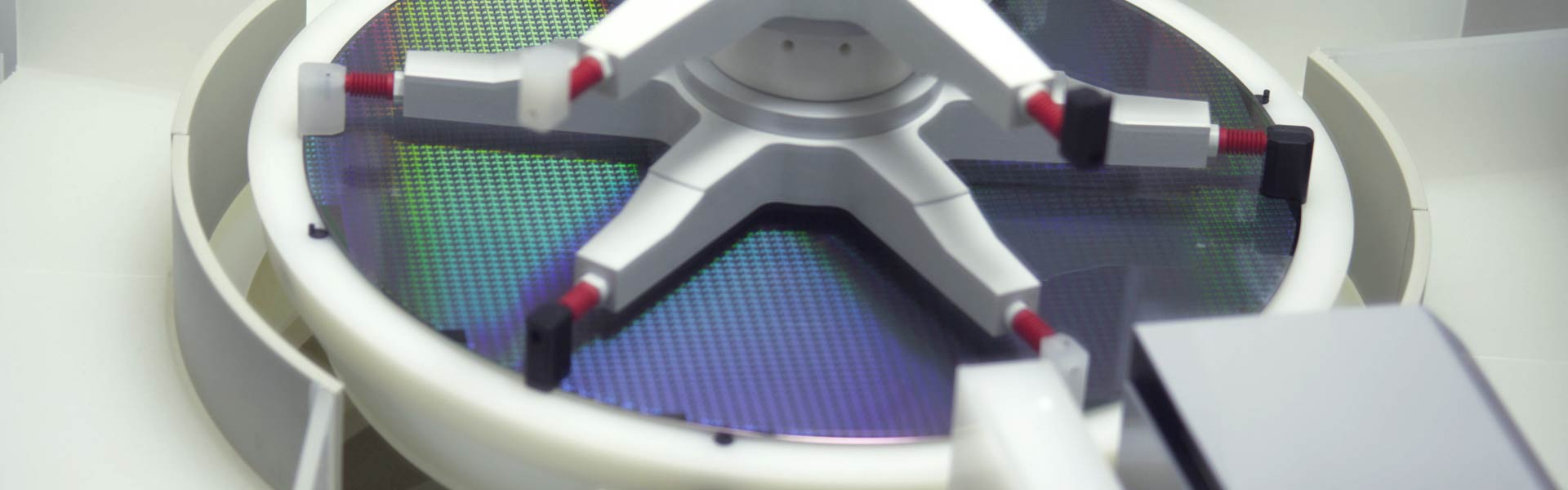
제조 전반에 걸쳐 웨이퍼 세정의 여러 단계를 높은 생산성으로 처리하는 데 필요한 공정 유연성을 갖추고 있습니다.
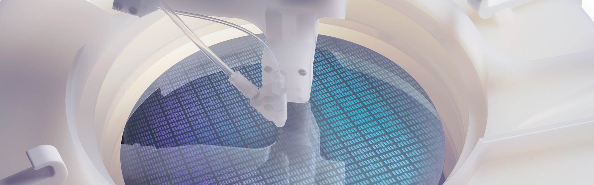
EOS 제품군
램리서치의 고급 습식 세정 제품은 점차 까다로워지는 고처리량 분야에서 온웨이퍼(on-wafer) 결함을 크게 줄입니다.

Fabtex™ Yield Optimizer
Fabtex™ Yield Optimizer is a cutting-edge software platform designed to help semiconductor foundries accelerate yield ramp and improve high-volume manufacturing performance.
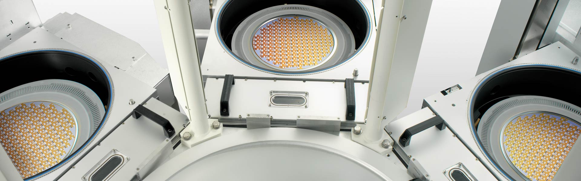
FLEX 제품군
램리서치의 유전체 식각 시스템은 용도에 맞춘 기능 덕분에 고급 소자의 까다로운 구조를 다양하게 만들 수 있습니다.
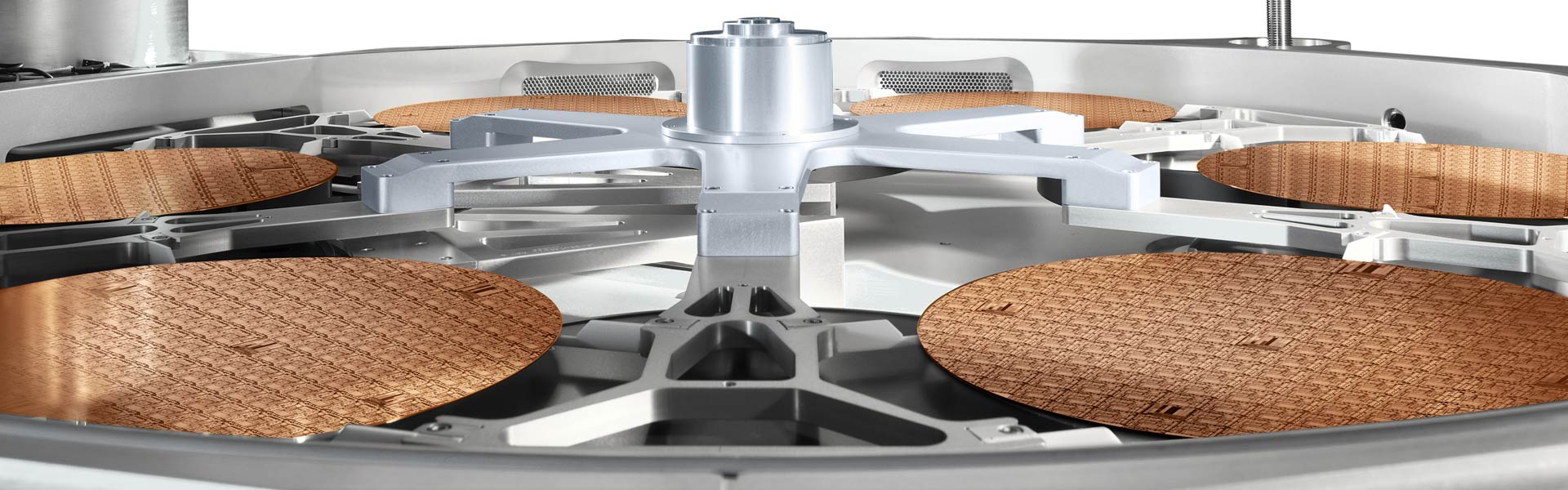
GAMMA 제품군
폭넓은 주요 포토레지스트 제거 분야에 필요한 공정 유연성을 갖췄습니다.

KIYO 제품군
시장을 선도하는 램리서치의 전도체 식각 제품은 주요 소자 피처(feature)에 요구되는 고성능 정밀도와 제어력이 특징입니다.
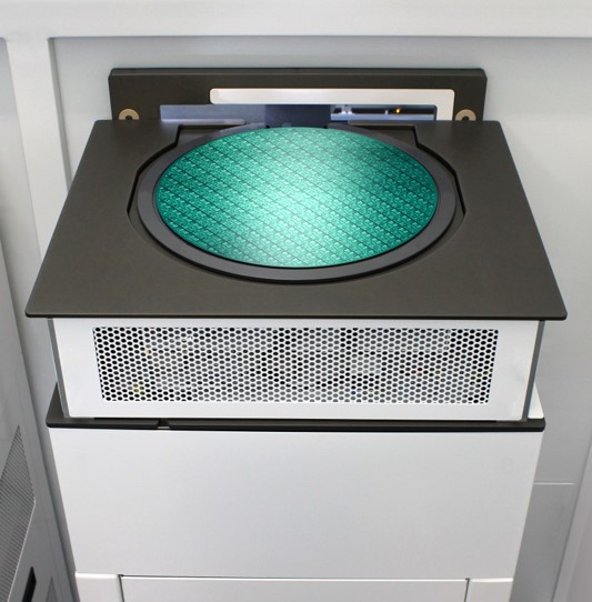
METRYX 제품군
램리서치의 질량 계측 시스템에는 3차원 소자 구조의 첨단 공정 모니터링과 제어에 필요한 밀리그램 미만 단위의 측정 기능이 있습니다.

OverViz
OverViz™는 플라즈마 방전의 높은 정확도(high-fidelity) 모델링을 위한 산업용 시뮬레이션 소프트웨어 플랫폼입니다.
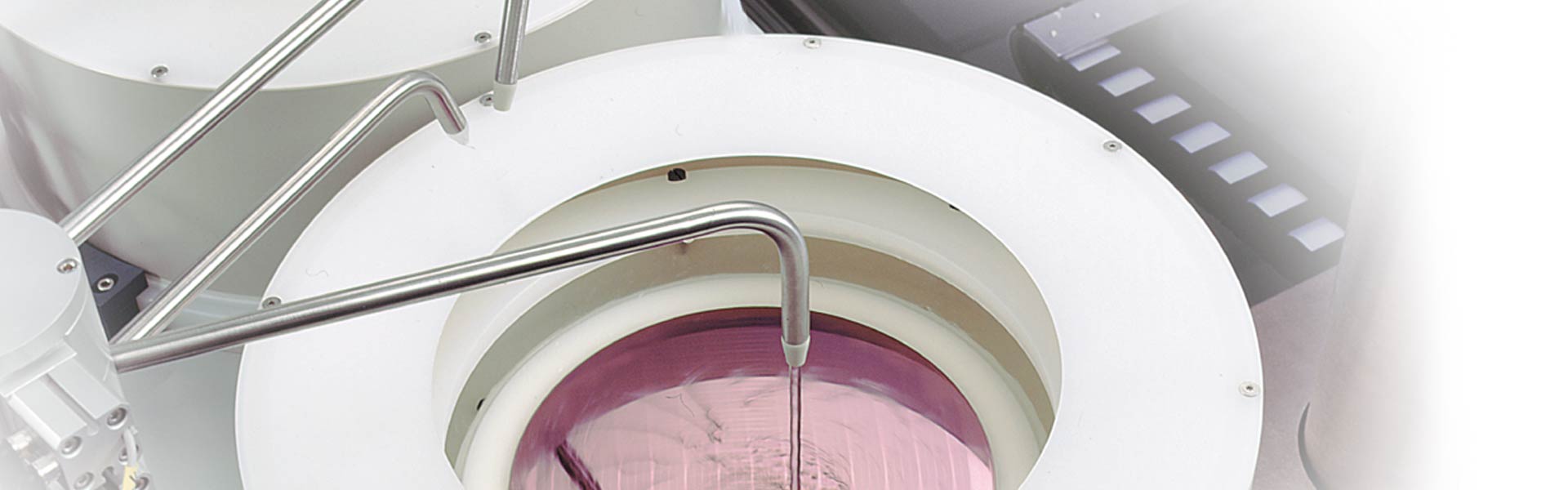
Reliant Clean 제품
램리서치의 Reliant 세정 제품군은 특수 기술의 로드맵을 지원하고 제조 시설의 생산 수명을 연장하는 솔루션을 제공합니다.
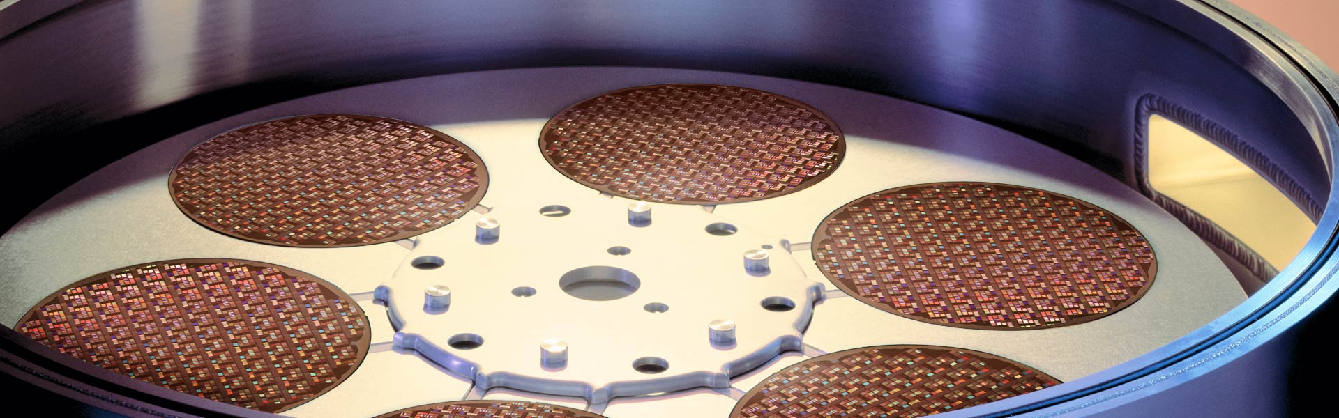
Reliant Deposition 제품
램리서치의 Reliant 증착 제품군은 특수 기술의 로드맵을 지원하고 제조 시설의 생산 수명을 연장하는 솔루션을 제공합니다.
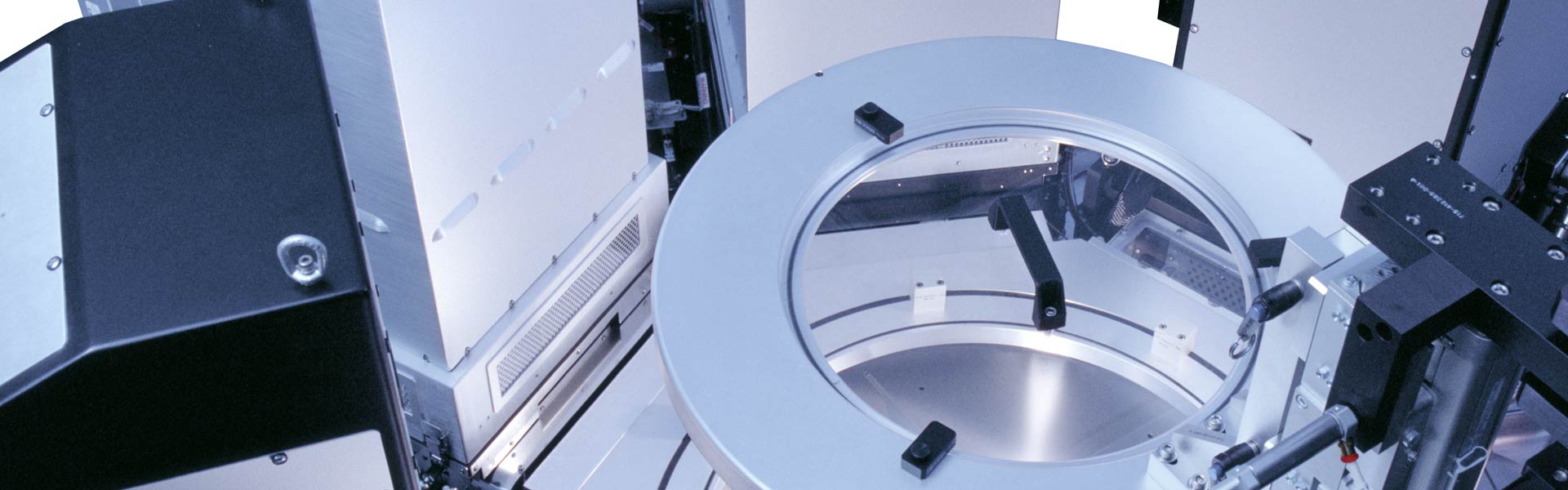
Reliant Etch 제품
램리서치의 Reliant 식각 제품군은 특수 기술의 로드맵을 지원하고 제조 시설의 생산 수명을 연장하는 솔루션을 제공합니다.
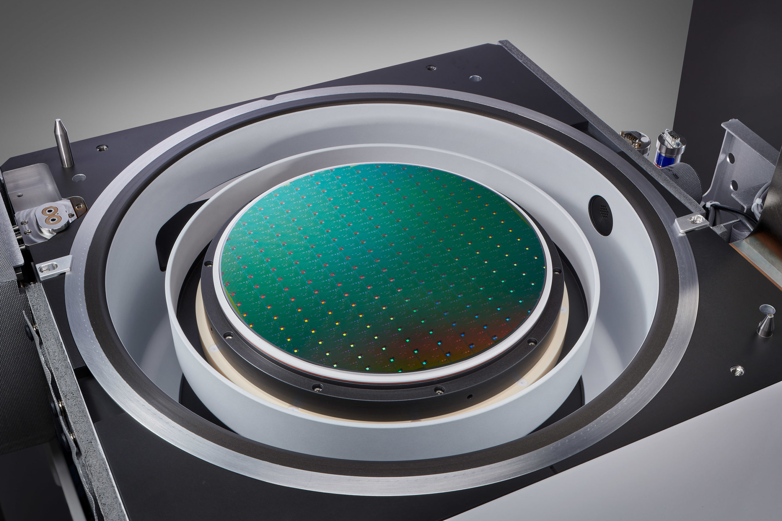
고선택비 식각 제품군
획기적인 고선택비 식각 장비 포트폴리오는 3D 구조와 첨단 로직 및 파운드리 애플리케이션을 위한 옹스트롬(Å) 수준의 정밀도와 초고도 선택비 기반의 역량으로 등방성 식각을 지원합니다.

SEMulator3D
SEMulator3D®는 광범위한 기술 개발 역량을 갖춘 반도체 공정 모델링 플랫폼입니다.
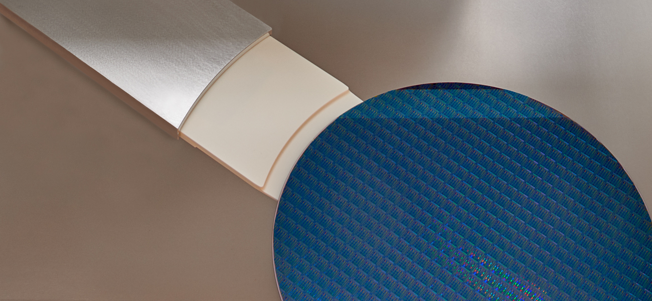
SENSE.I 제품군
램리서치의 최신 식각 플랫폼은 컴팩트한 고밀도 구조에 누구도 따라올 수 없는 시스템 지능을 갖추고 있어 공정 성능을 최고의 생산성으로 구현합니다.
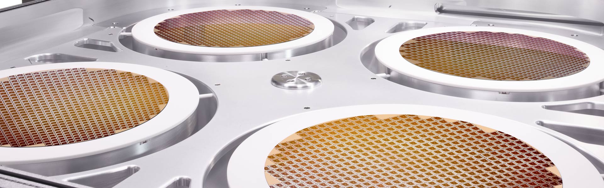
SOLA 제품군
이 제품군은 박막의 특수 증착 후처리를 통해 첨단 박막 분야에 필요한 물리적 특성을 개선합니다.
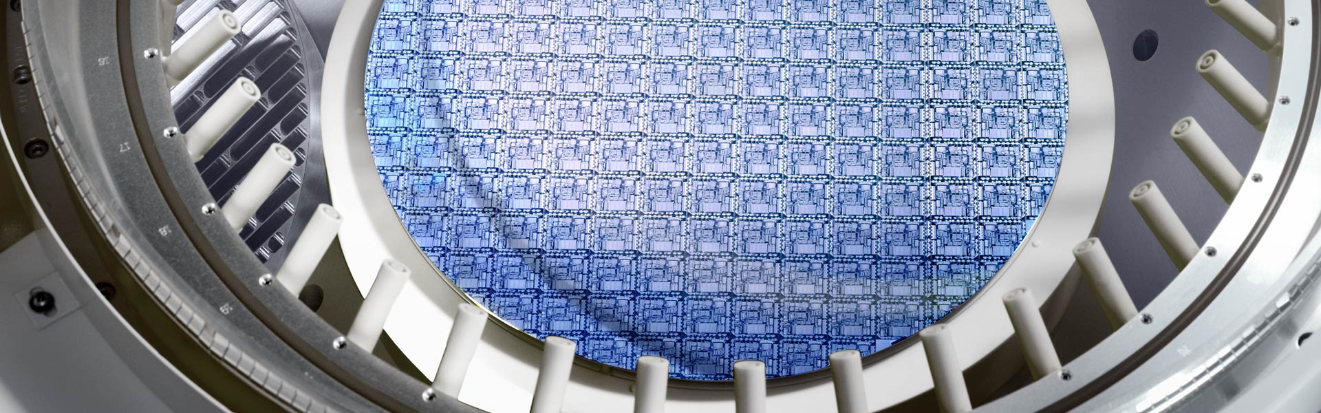
SPEED 제품군
이 유전체 증착 제품은 업계 최고의 처리량과 신뢰성으로 고종횡비(high aspect ratio) 공간에 완벽한 갭필(gapfill)을 구현합니다.
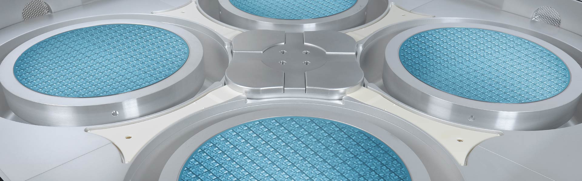
Striker 제품군
첨단 ALD 기술을 사용하여 나노 수준의 피처가 있는 고급 소자의 주요 공정을 완벽하게 제어하는 유전막을 제공합니다.
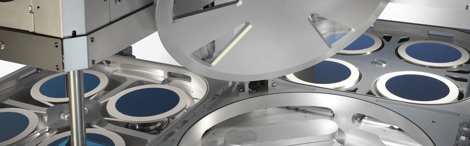
VECTOR 제품군
램리서치의 PECVD 제품군은 광범위한 소자 분야에서 높은 생산성으로 고정밀 유전막 증착을 실현합니다.
Related Blog Posts
Understanding CFETs, a Next Generation Transistor Architecture
Computing power has experienced exponential growth over the last 70 years. This has largely been achieved through transistor scaling. Due to a continuous reduction in the size of transistors, engineers have been able to pack more and more of them onto a single chip[1]. This has led to faster, more powerful, and more energy-efficient devices. Improvements in fabrication processes and materials, along with better circuit design techniques, have enabled this scaling. As transistors have become smaller and more densely packed, we have started to reach limitations caused by the laws of physics.
Improving Gate All Around (GAA) Transistor Performance using Virtual Process Window Exploration
As transistor sizes shrink, short channel effects make it more difficult for transistor gates to turn a transistor ON and OFF [1]. One method to overcome this problem is to move away from planar transistor architectures toward 3D devices. Gate-all-around (GAA) architectures are an example of this type of 3D device [2]. In a GAA transistor, the gate oxide surrounds the channel in all directions. A key process during the fabrication of GAA transistors involves the channel release step.