Virtually every leading edge device has been made using our equipment
Advanced microchips are in many of the familiar products we use every day – from mobile phones and computing devices to entertainment systems and increasingly “smart” cars. Electronic products are everywhere and life without them is unimaginable.
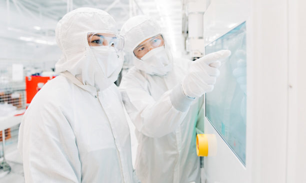
Creating the tiny, complex chips used in these devices involves the repetition of a core set of processes and includes hundreds of individual steps. For successful production, semiconductor manufacturers require sophisticated processes and fabrication equipment.
We work closely with customers to deliver the products and technologies needed to enable their success. By offering critical chip-processing capabilities, our products provide a vital link between the visionary designs for the latest electronic devices and the companies that produce them.
Our solutions
Market demand for faster, smaller, more powerful, and energy-efficient electronics is driving the development of new fabrication strategies that enable producing advanced devices with fine, closely packed features and complex 3D structures. Creating the cutting-edge microprocessors, memory devices, and numerous other product types in demand today is extremely challenging and requires continuous innovation to deliver capable processing solutions.
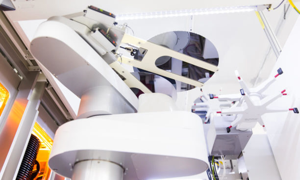
Through collaboration and drawing on multiple areas of expertise, Lam continues to develop the new capabilities required to manufacture these increasingly challenging devices. Our innovative technology and productivity solutions deliver a wide range of wafer processing capabilities needed to create the latest chips and applications – from transistor, interconnect, patterning, advanced memory, and packaging to sensors and transducers, analog and mixed signal, discretes and power devices, and optoelectronics and photonics.
Our processes
Semiconductor processes used in the manufacture of today’s most advanced chips are challenged to literally push the limits of physics and chemistry with their nanoscale features, novel materials, and increasingly complex 3D structures. Meeting the ever-changing fabrication demands of new chip designs requires precision control at the atomic scale.
To ensure those new process technologies are production-ready when new chips head to the fab, our scientists and engineers stay abreast of our customers’ manufacturing needs. Our broad portfolio of market-leading products for thin film deposition, plasma etch, photoresist strip, and wafer cleaning are complementary processing steps used throughout semiconductor manufacturing. To support advanced process monitoring and control of critical steps, our product offerings include a line of high-precision mass metrology systems.