Products
Kiyo Product Family
Reactive Ion Etch (RIE)
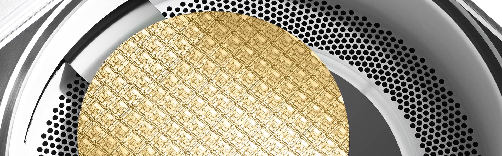
Conductor etch helps shape the electrically “active” materials of a semiconductor device. Even a slight variation in these miniature structures can degrade device performance. In fact, these structures are so tiny and sensitive that etch processes push the boundaries of the basic laws of physics and chemistry.
Lam’s Kiyo® product family delivers the high-performance capabilities needed to precisely and consistently form these features precisely and with high productivity. For some applications, select models are also available through our Reliant® Systems as refurbished products, providing lower cost of ownership with the same quality assurance and performance as new systems.
As the semiconductor industry continues to shrink critical feature sizes and improve device performance, conductor etch challenges include processing smaller features, new materials, and new transistor structures on the wafer. Due to decreasing feature sizes, the etch process requires atomic-level control not only for each feature, but also across the entire wafer. Metal gates and high-k dielectric materials in the device stack need advanced multi-film etching capability. Leading-edge chip designs require etching structures such as recessed channel and 3D gate transistors, as well as conventional planar transistors. Furthermore, double and quadruple patterning techniques to address lithography limitations at the sub-20 nm nodes require the etch process to define the pattern on the wafer as well as reproduce it.