Products
Sense.i Product Family
Reactive Ion Etch (RIE)
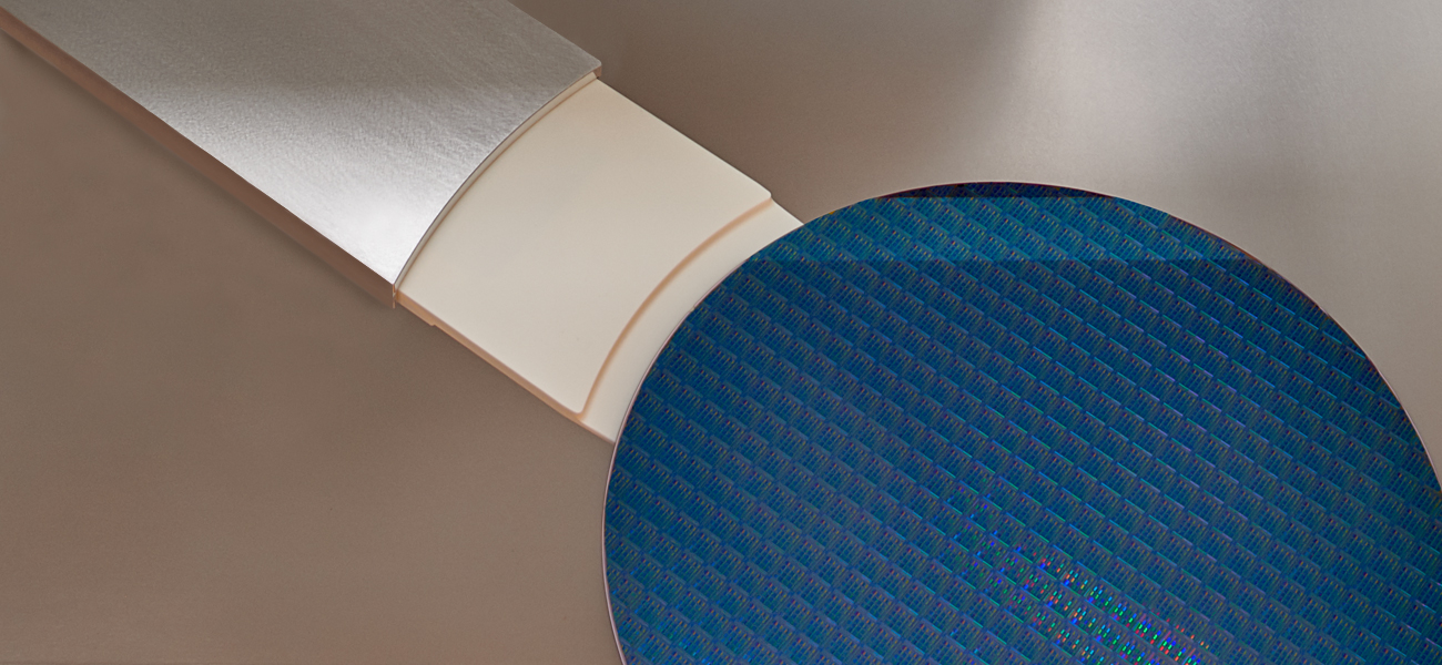
Plasma etch selectively removes material to create desired features and patterns of a semiconductor device. As devices continue to scale, precise and repeatable etching is needed to achieve the required feature characteristics. Sensitive new materials and complex architectures pose additional challenges.
With technology evolved from our industry-leading Kiyo® and Flex® process modules, the Sense.i® product family delivers the high-performance capabilities needed to precisely and consistently form these features.
Sense.i® offers differentiated technologies and application-focused capabilities for critical and semi-critical etch applications. The new system architecture also delivers the productivity and repeatability required to support logic and memory device roadmaps well into the coming decade and beyond.
As the semiconductor industry continues to drive device performance and cost scaling, there is an ever-growing need for innovation in device process capability and extendibility. Device roadmaps depend on critical device features, often in 3D, and drive the need to etch smaller features, new materials, and new transistor structures on the wafer. In addition, the ability to etch multi-layer film stacks, often with extreme selectivity from one film to another, while creating optimal etched profiles at increasingly higher aspect ratios will be required.
The technical challenges of the devices require innovation in high volume manufacturing as well. As etch process times increase, the need to optimize the factory output is growing. Smarter and denser tools are required to enable the industry to transform their manufacturing practices and to adopt standards that increase efficiency and output.