Products
VECTOR Product Family
Plasma-Enhanced Chemical Vapor Deposition (PECVD)
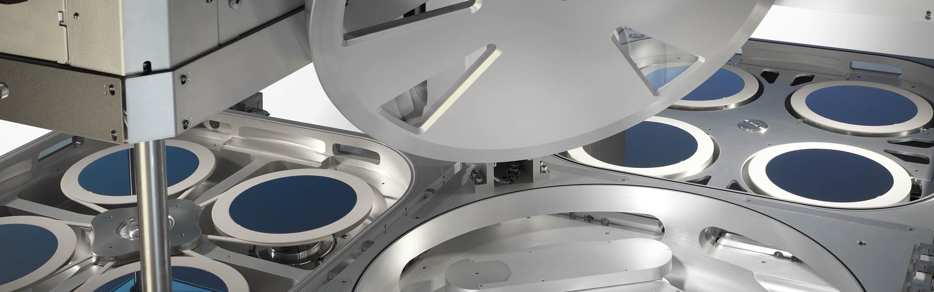
Dielectric film deposition processes are used to form some of the most difficult-to-produce insulating layers in a semiconductor device, including those used in the latest transistors and 3D structures. In some applications, these films need to conform tightly around intricate structures. Other applications require dielectric films to be exceptionally smooth and defect free since slight imperfections are multiplied greatly in subsequent layers.
Lam’s VECTOR® PECVD products are designed to provide the performance and flexibility needed to create these enabling structures within a wide range of challenging device applications. For some applications, select models are also available through our Reliant® Systems as refurbished products, providing lower cost of ownership with the same quality assurance and performance as new systems.
As feature dimensions in advanced semiconductors continue to shrink, many critical process steps rely on the deposition of exceptionally high-quality dielectrics – smooth, void-free films that meet exacting thickness, feature coverage, mechanical stress, and electrical requirements. PECVD technology is often used for these processes. For example, in 3D NAND designs, in-situ PECVD deposition of well over 100 pairs of alternating film layers requires the capability to closely control stress and defectivity of each individual layer while depositing perfectly flat, multi-layer structures. Another key application is hardmask films – sacrificial layers that enable precise patterning when conventional masks fail. Here, ultra-smooth and uniform films are needed to avoid compounding errors over many passes, while good film mechanical strength helps to avoid line pattern collapse in very high aspect ratio features. To address these diverse and challenging requirements, deposition equipment must provide flexibility for a wide range of process applications, while maintaining high productivity and low cost.