Products
Phoenix Product Family
Electrochemical Deposition (ECD)PR-DevelopmentPR-StripWet Clean/Strip
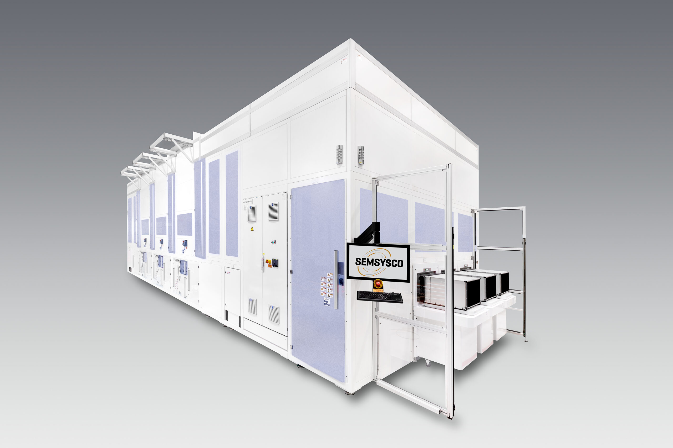
Phoenix offers a fully-automated high volume panel processing for 510x515mm substrates.
Designed with the goal to redefine cost of ownership, Phoenix delivers unique technologies in the panel level packaging industry together with a respectful usage of its operating utilities.
Inspired by wafer level performance Phoenix offers strip, development, etch and plating solutions to address the future market requirements driven by AI, high performance computing and other applications.
Advanced packaging is becoming an increasingly critical approach to continue scaling beyond silicon. Several device manufacturers and fabless companies are increasing adoption of novel chiplet solutions to meet level performance and cost requirements. This accelerating chiplet transition requires new packaging solutions and innovations in the substrate market segment. As traditional silicon scaling approaches cost and technology limitations, companies are adopting novel chiplet and heterogenous integration solutions. To ensure continued scaling, substrate solutions require several innovations in process equipment solutions. In addition to meeting the technology roadmap needs, substrate level equipment must have increased flexibility to process panels of various materials and sizes. In addition, high productivity and low cost of ownership are desirable for high volume manufacturing environments.