Products
GAMMA Product Family
Dry Strip
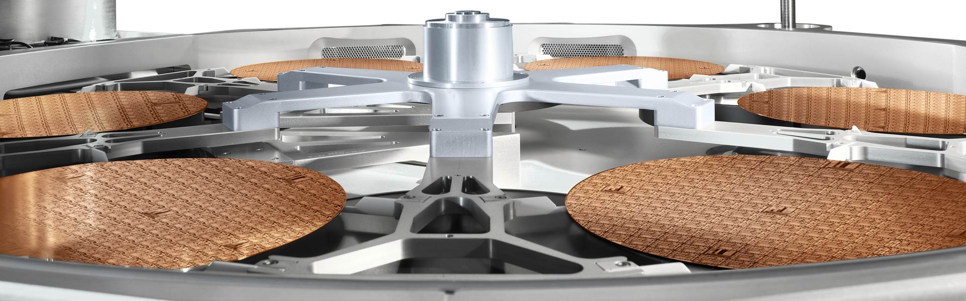
Strip processes remove photoresist and various residues left behind by other processes. Downstream plasma processes are also used to condition the wafer surface to give it certain properties necessary for subsequent processing. Critical to final device performance, strip processes must ensure minimal impact to feature shapes (CDs) and minimal to zero device materials loss.
Lam’s production-proven GAMMA® product family systems with a broad range of downstream plasmas provide the process flexibility needed for a range of critical wafer processing applications.
With the semiconductor industry’s migration to ultra-shallow junctions, multiple patterning, ultra low-k dielectrics, and 3D architectures, photoresist strip processes need to deal effectively with more complex device structures. At the transistor level, small changes in the film as a result of the strip process can affect junction resistivity, junction depth, and dopant activation, thereby affecting device performance. For interconnect structures, unwanted changes in the properties of low-k dielectrics can also impact performance. Photoresist removal can also negatively impact materials used in advanced memory applications. These concerns are driving the development of new strip processes for advanced technology nodes. Challenges include removing residues, minimizing oxidation and silicon loss, and providing damage-free results, while at the same time delivering high throughput and low cost of ownership.