SEMulator3D
Products
Semiconductor Process Modeling
Industry Challenges
Continued semiconductor technology advancement into 3D processes, including Gate-All-Around FET, 3D Memory, BEOL and backside patterning, has significantly increased the complexity of process development. As a result, the traditional build-and-test approach to technology development has become excessively costly and time-consuming.
With state-of-the-art fabs requiring multi-billion dollar investments, and technology growing ever more complex, the time and cost of trial-and-error silicon engineering have become unacceptable. The concurrent penalty for missing a market window has become extreme. Predictive, 3D process modeling with Coventor’s semiconductor process modeling software is an alternative approach that can dramatically reduce silicon learning cycles, cut development costs, and reduce the risk of missing a market window. Unlike actual wafer runs, which take weeks to month, virtual fabrication takes minutes to hours to produce results.
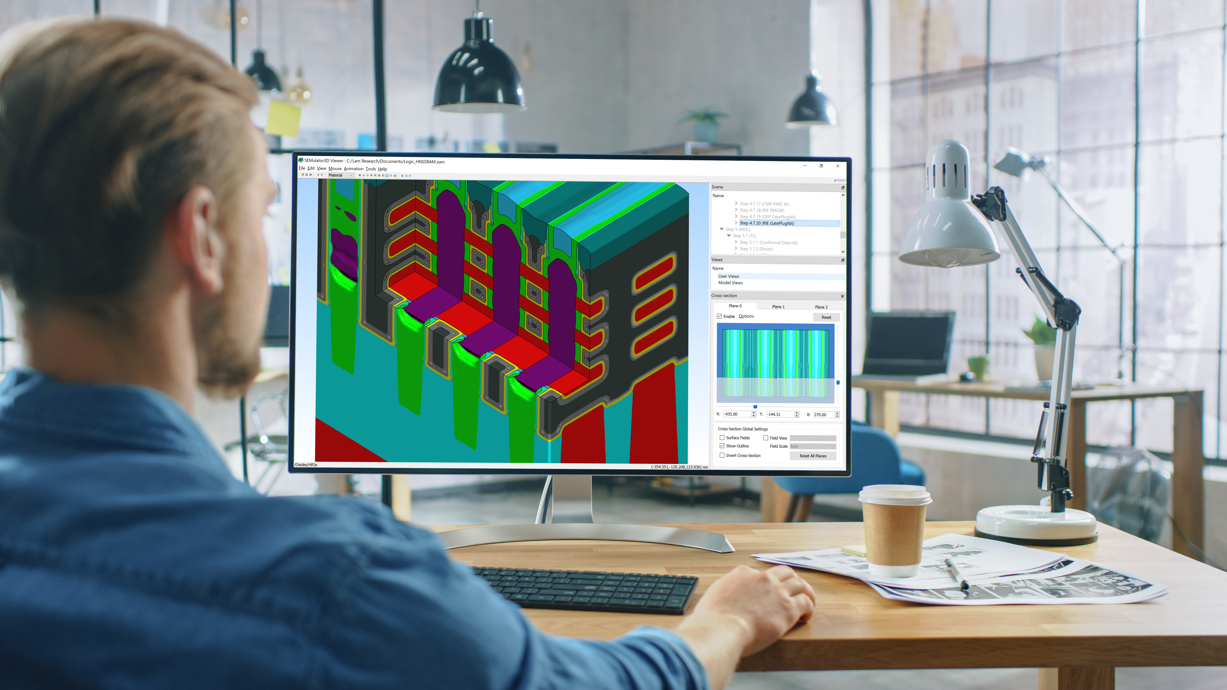
Predictive 3D process modeling with Coventor’s SEMulator3D virtual fabrication platform reduces development cycle time and costs associated with traditional silicon experimental learning. SEMulator3D enables companies to bring new technologies to volume production sooner by leveraging virtual fabricated wafers for development.
Key Customer Benefits
- Time – Hours and days to solution via simulation versus weeks and months with real silicon
- Cost – Reduction in requirement for capital equipment, engineering & factory staff, wafers, masks, chemicals, consumables & facilities
Product Offerings
- SEMulator3D®
Key Applications
-
Pathfinding
-Process integration validation
-Big Branch decisions
-Process assumptions -
Defect Analysis
-3D Failure Checks
-Defect Kill Ratio
-R/C, Leakage, Device, IV, CV, etc. -
Yield: Ramp and HVM
-Design Process Optimization
-Process Window Optimization
-Cross-Wafer Uniformity