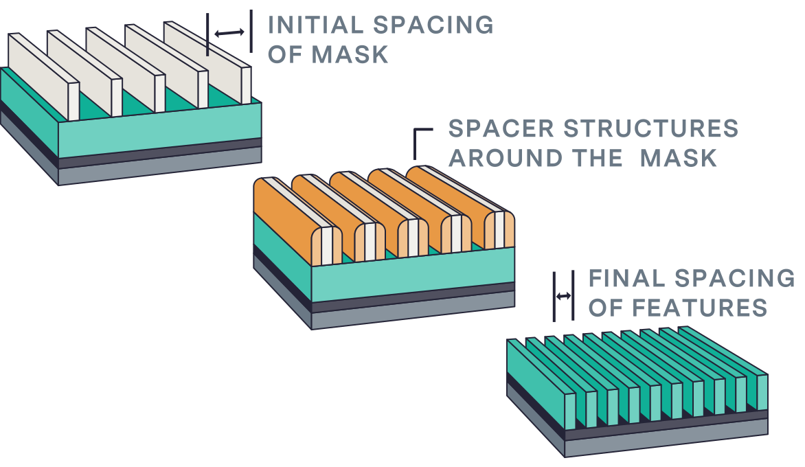
パターニングは露光(リソグラフィ)、成膜、エッチングの3つのステップから成り、ICを構成する極微小で複雑なパターンを形成する工程です。技術世代が新しくなる度にデバイスのパターン寸法は小さくなります。最先端のデバイスではパターン寸法や隣接パターンとの間隔が狭くなりすぎて、従来のリソグラフィ(マスクと呼ばれる原板に描かれた微細パターンをウェハに露光転写する工程)では対応出来なくなっています。これを補うために、半導体メーカはダブル/4重パターニングやスペーサ式パターニングなどの高度な手法を用いています。ここでは一層のパターン形成に複数枚のマスクを使用し、露光・成膜・エッチングの3点セットを複数回繰り返す必要があるのです。これで確かにリソグラフィの制約は緩和されるのですが、その一方で、精細で高密度のパターンを正確に形成するためには、これまでなく高度なプロセス精度と薄膜品質が求められるようになっています。
ラムリサーチのソリューション
パターニング
CORONUSシリーズ製品
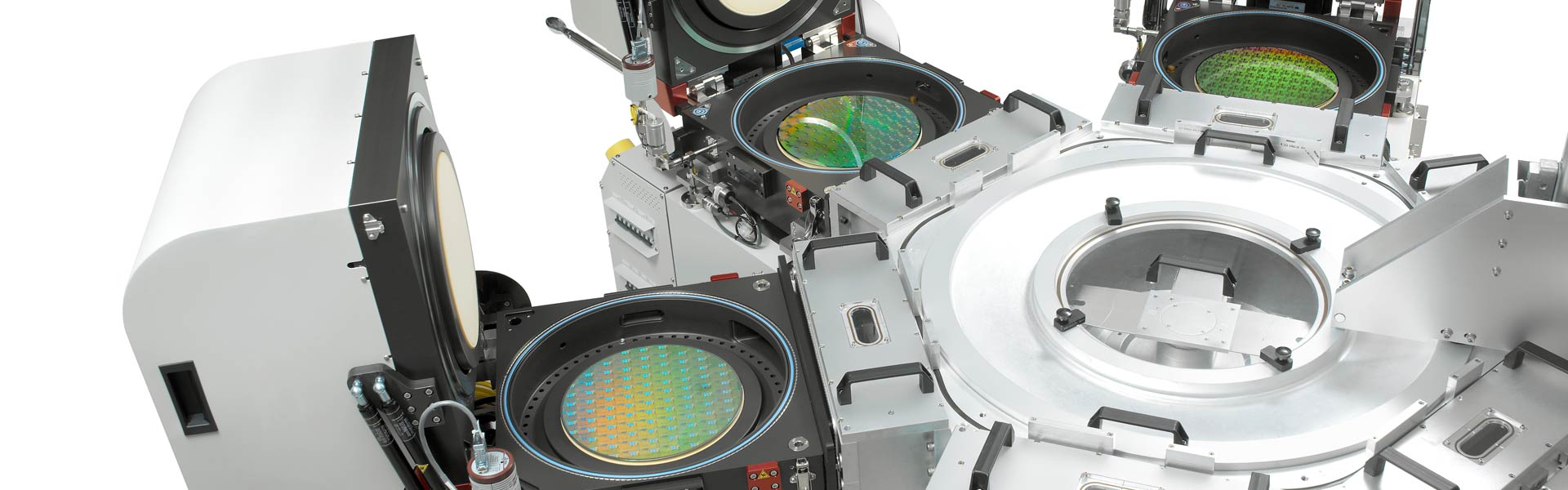
半導体製造工程全体の歩留まりを向上させるためにCoronus システムはウェハのベベルエッジに着目しました。半導体製造工程を通じてウェハエッジ部には残渣や残膜 やラフネスが蓄積します。これが剥がれ落ちて他の場所に付着すると欠陥となり、デバイス不良を引き起こす原因なります。Coronus エッチはベベルの残渣を除去し、Coronus デポジションはベベルをダメージから保護する製品です。

DV-PRIME & DA VINCI シリーズ
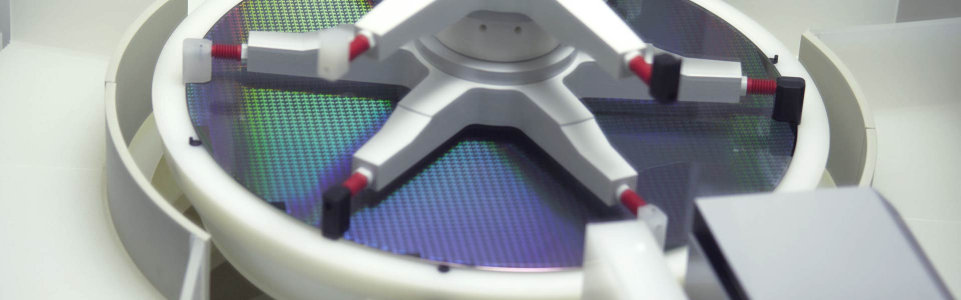
これらの製品は製造工程全体にわたる複数のウェハクリーニングステップにおいて求められる高い生産性と柔軟性を実現するプロセスを提供します。
EOS シリーズ製品
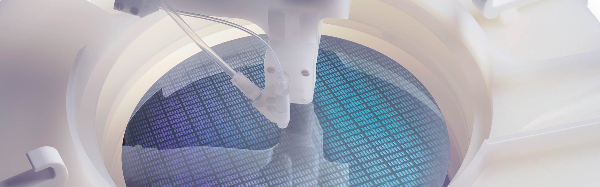
ラムリサーチの先進的なウェットクリーン製品は、厳しい要求条件の用途に対して高スループットで不良率が低いウェハ生産を可能にします。

Fabtex™ Yield Optimizer
Fabtex™ Yield Optimizer is a cutting-edge software platform designed to help semiconductor foundries accelerate yield ramp and improve high-volume manufacturing performance.
FLEX シリーズ製品
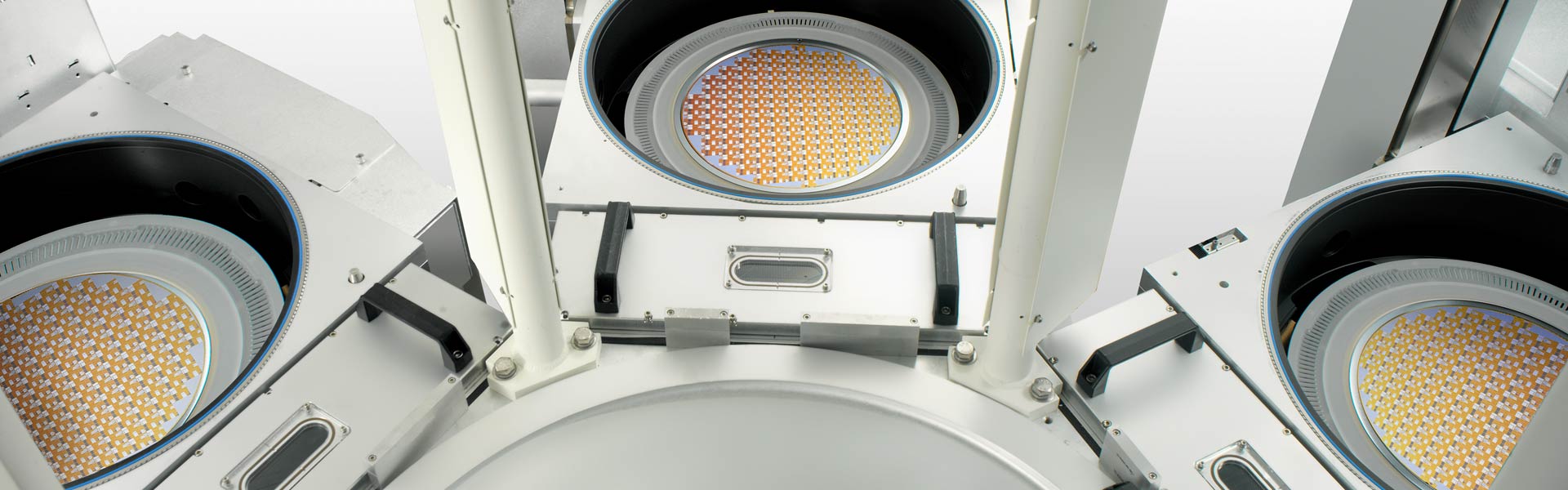
ラムリサーチの酸化膜エッチシステムは、先進のデバイスに求められる複雑な構造を備えた幅広いアプリケーションに配慮した機能を提供します。
GAMMAシリーズ製品
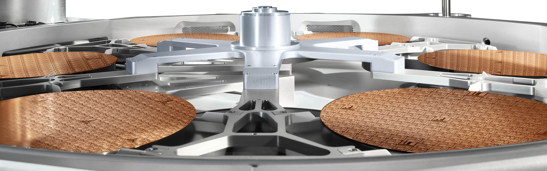
これらの製品は、各種のクリティカルなフォトレジスト ストリップ アプリケーションに対応した高いプロセス柔軟性を提供します。
KIYO シリーズ製品
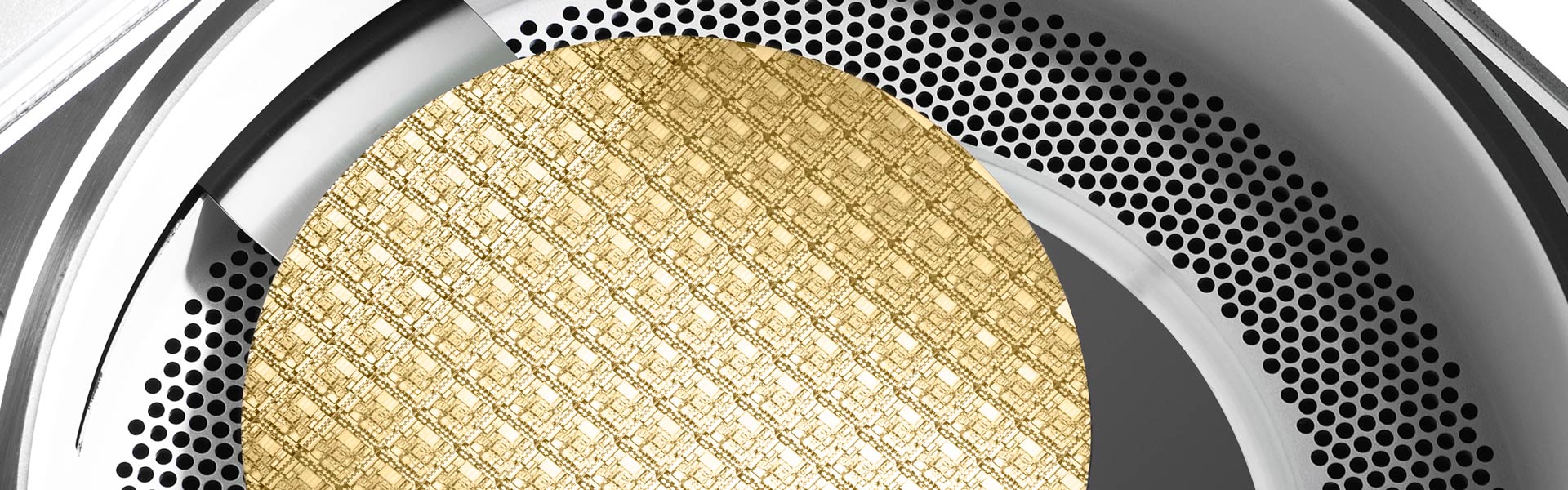
業界をリードするコンダクターエッチング製品は、クリティカルなデバイス機能に必要な高精度と高い生産性での制御を実現します。
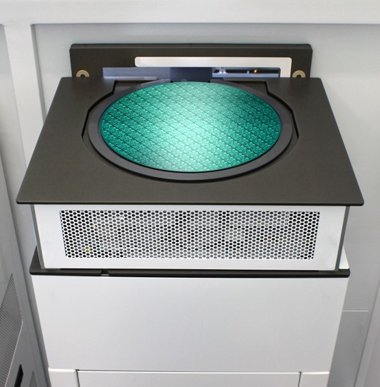
METRYX シリーズ製品
ラムリサーチの質量計測システムは、高度なプロセス監視と3次元デバイス構造の制御により、サブミリグラムレベルの計測能力を提供します。
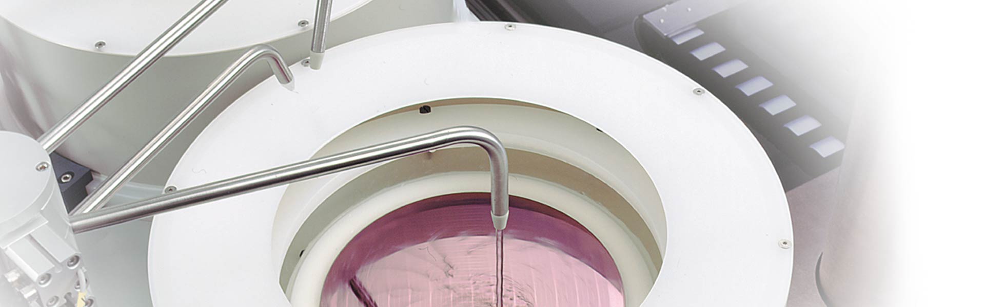
RELIANT クリーニング製品
ラムリサーチの RELIANTクリーニング製品は、スペシャルティ・テクノロジーのロードマップを実現し、ファブの生産寿命を延ばします。
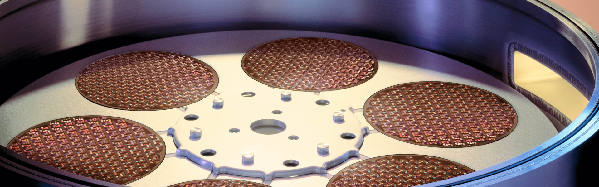
RELIANT成膜製品
RELIANT 成膜製品は、スペシャルティ・テクノロジーのロードマップを実現し、ファブの生産寿命を延ばします。
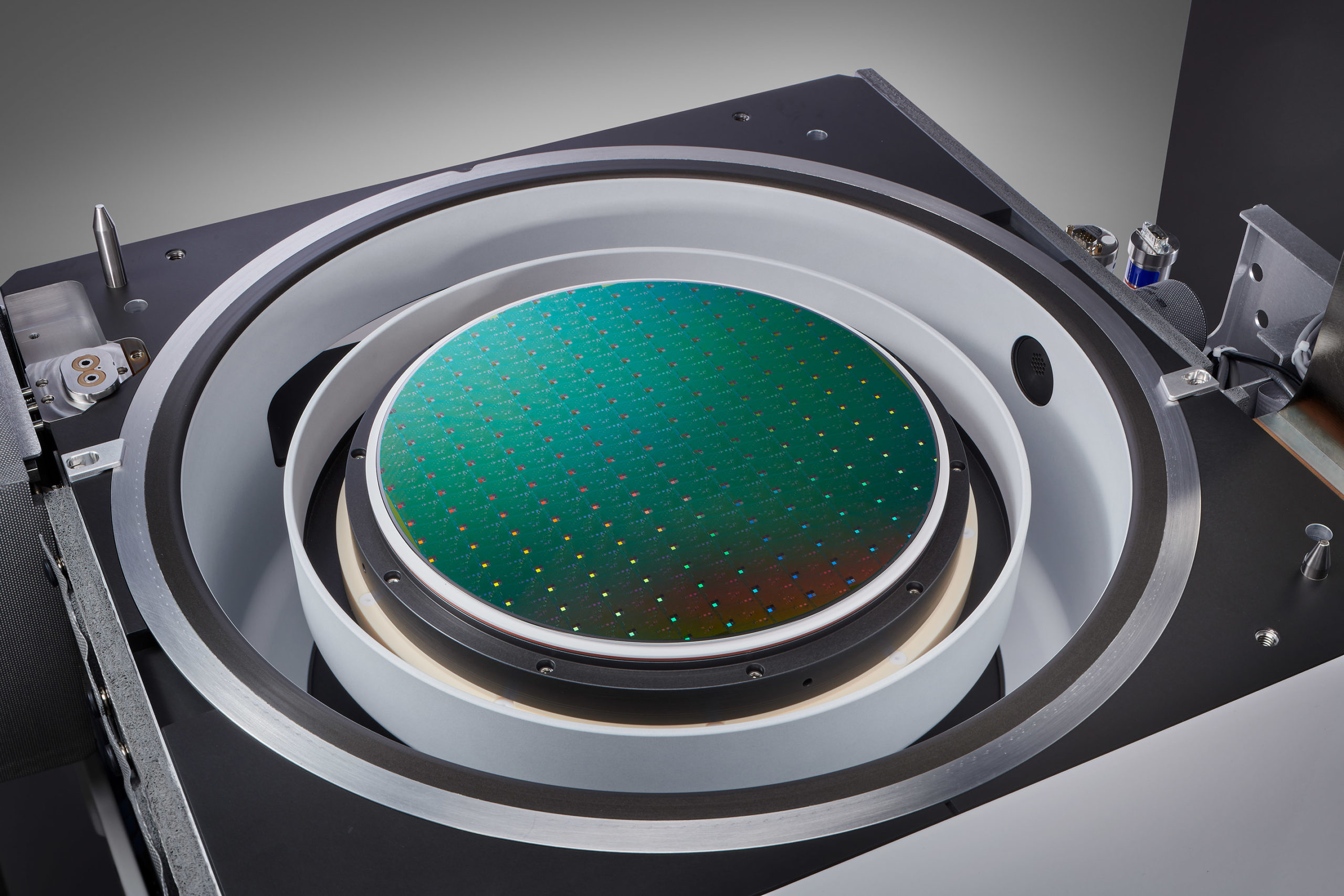
高選択エッチング製品群
画期的なポートフォリオにより、3D アーキテクチャ、先端ロジックおよびファウンドリ用途向けに、0.1nm スケールの精度と超高選択性で等方的材料除去を実現します。
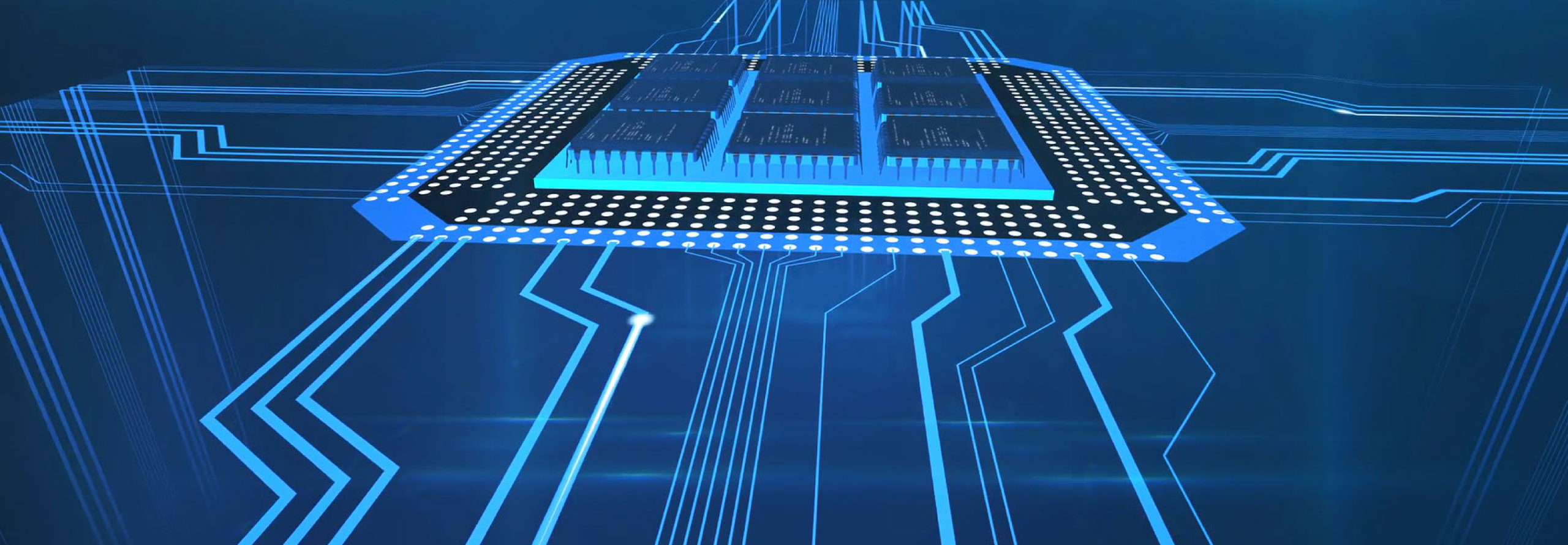
SEMulator3D
半導体プロセスモデリング・プラットフォーム SEMulator3D® は広範囲にわたる技術開発環境を提供します。
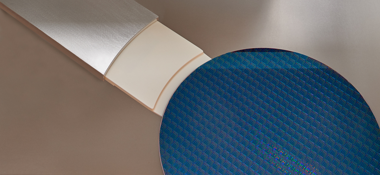
SENSE.I製品
私たちの最新エッチング装置のプラットフォームは、最高の生産性でプロセスパフォーマンスを提供するコンパクトで高密度のアーキテクチャで比類のないシステムインテリジェンスを実現します。
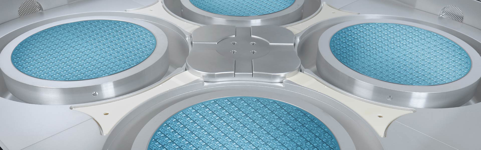
STRIKER シリーズ製品
高度なALD技術を活用することにより、これらの製品はナノスケールの機能を備えた高度なデバイスのクリティカルプロセスに対して優れた制御性能を実現する酸化膜を提供します。
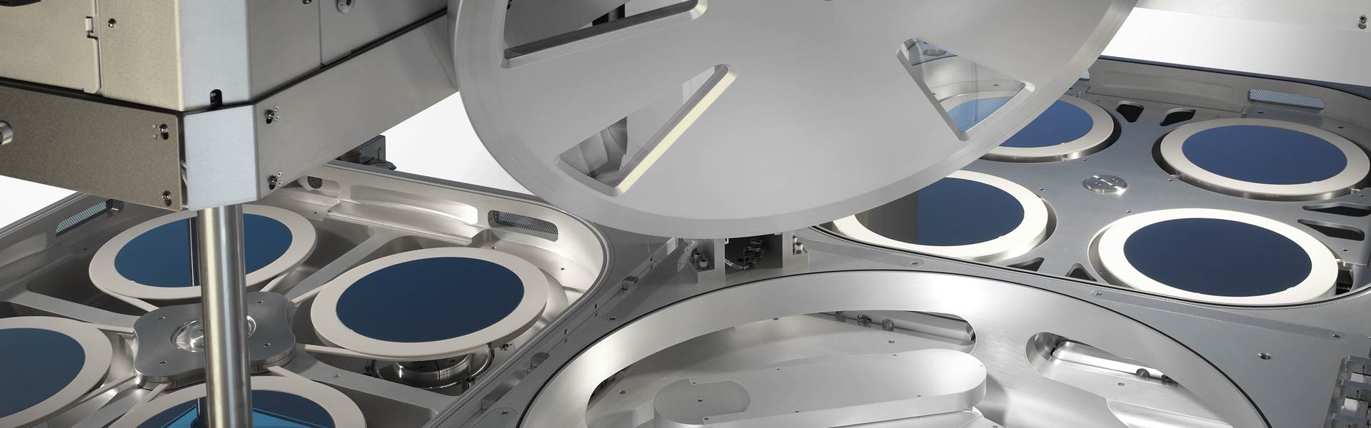
VECTOR シリーズ製品
ラムリサーチ社のPECVD製品ファミリーは、幅広いデバイスアプリケーションに対応した高い生産性の精密な酸化膜成膜を提供します。
VERSYS METAL シリーズ製品
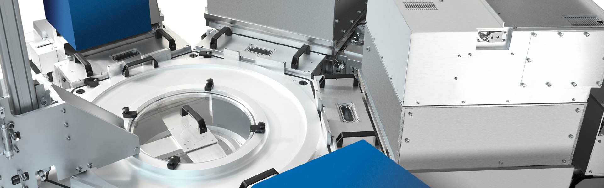
これらのメタルエッチング製品は、電気配線およびメタルハードマスク用途向けに高い生産性を備えたプロセス制御を提供します。
Related Blog Posts

Improving Line Edge Roughness Using Virtual Fabrication
Line edge roughness (LER) is a variation in the width of a lithographic pattern along one edge of a structure inside a chip. Line edge roughness can be a critical variation source and defect mechanism in advanced logic and memory devices, and can lead to poor device performance or even device failure [1~3]. Deposition-etch cycling is an effective technique to reduce line edge roughness. In this study, we demonstrate how virtual fabrication can provide guidance on how to perform deposition/etch cycling in order to reduce LER.
Virtual Exploration of Novel Vertical DRAM Architectures
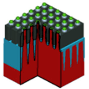
In this article, we demonstrate a pathfinding technique for a novel Vertical DRAM technology. First, we identify important process parameters (defined by current semiconductor production equipment capabilities) that strongly impact yield. By using a virtual model, we then perform experimental optimization of the Vertical DRAM device across specific target ranges, to help predict and improve the yield of this next generation product.