
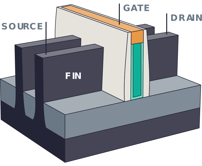
チップの「頭脳」たるトランジスタは電気の流れを制御する微小なスイッチです。一つのICに文字通り何10億個ものトランジスタが乗っています。より小さく、よりパワフルな電子機器を求める需要の高まりに促され、3D FinFET のような新しい構造のトランジスタや High-kゲート絶縁膜/メタルゲートのような新材料が開発されています。それにより、更なる微細化の進展が可能になっているのです。最新世代のトランジスタ寸法は原子数個分にまで来ており、それ故に製造は困難を極めます。こうした先端デバイスが設計意図通りの性能を発揮できるよう製造するには、並外れた制御精度で微細加工を行う能力が必要なのです。
ラムリサーチのソリューション
トランジスタ
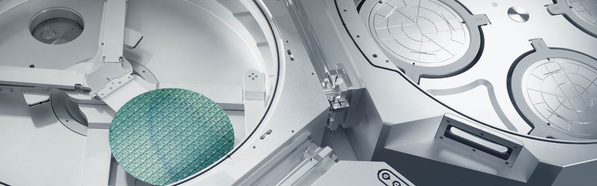
ALTUS製品ファミリー
CVDとALD技術を組み合わせた市場をリードするこれらのシステムにより、先進的なタングステンメタライゼーション用途向けに高コンフォーマルな金属膜を成膜します。

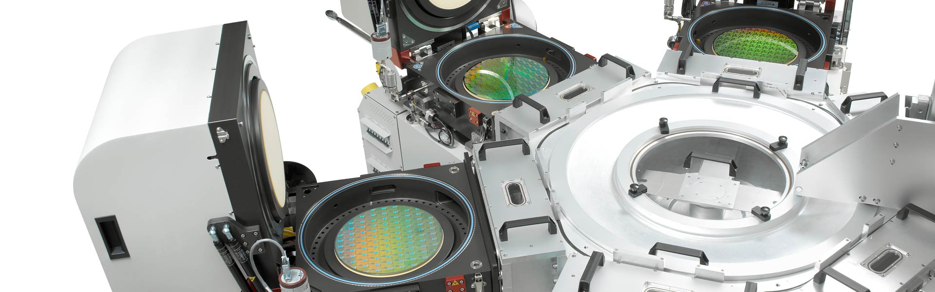
CORONUSシリーズ製品
半導体製造工程全体の歩留まりを向上させるためにCoronus システムはウェハのベベルエッジに着目しました。半導体製造工程を通じてウェハエッジ部には残渣や残膜 やラフネスが蓄積します。これが剥がれ落ちて他の場所に付着すると欠陥となり、デバイス不良を引き起こす原因なります。Coronus エッチはベベルの残渣を除去し、Coronus デポジションはベベルをダメージから保護する製品です。
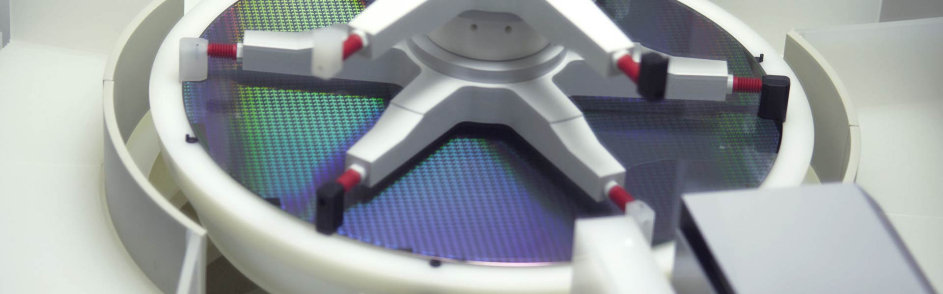
DV-PRIME & DA VINCI シリーズ
これらの製品は製造工程全体にわたる複数のウェハクリーニングステップにおいて求められる高い生産性と柔軟性を実現するプロセスを提供します。
EOS シリーズ製品
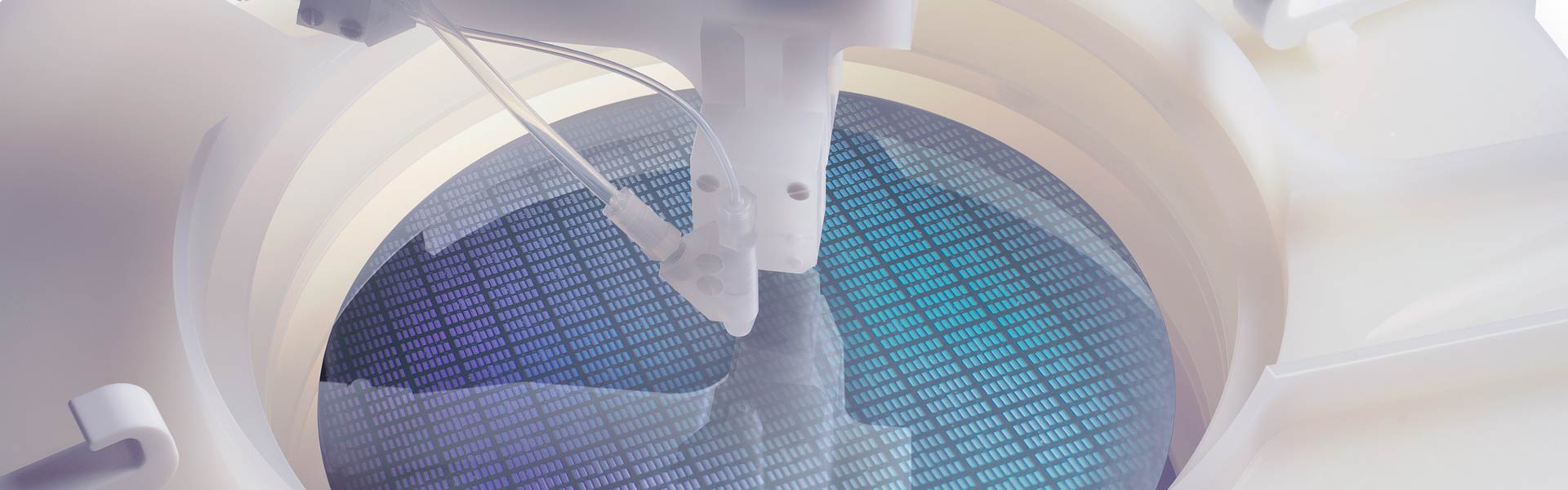
ラムリサーチの先進的なウェットクリーン製品は、厳しい要求条件の用途に対して高スループットで不良率が低いウェハ生産を可能にします。

Fabtex™ Yield Optimizer
Fabtex™ Yield Optimizer is a cutting-edge software platform designed to help semiconductor foundries accelerate yield ramp and improve high-volume manufacturing performance.
FLEX シリーズ製品
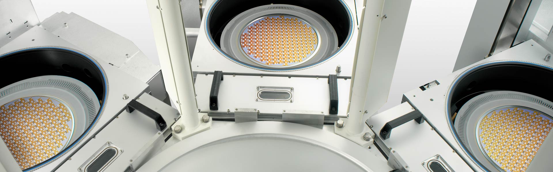
ラムリサーチの酸化膜エッチシステムは、先進のデバイスに求められる複雑な構造を備えた幅広いアプリケーションに配慮した機能を提供します。
GAMMAシリーズ製品
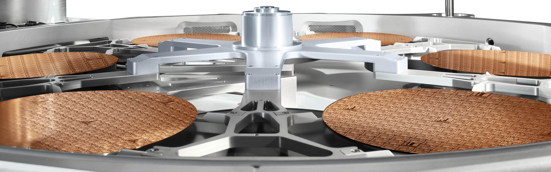
これらの製品は、各種のクリティカルなフォトレジスト ストリップ アプリケーションに対応した高いプロセス柔軟性を提供します。
KIYO シリーズ製品
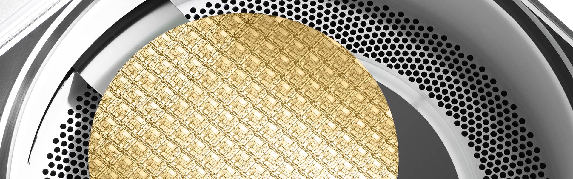
業界をリードするコンダクターエッチング製品は、クリティカルなデバイス機能に必要な高精度と高い生産性での制御を実現します。
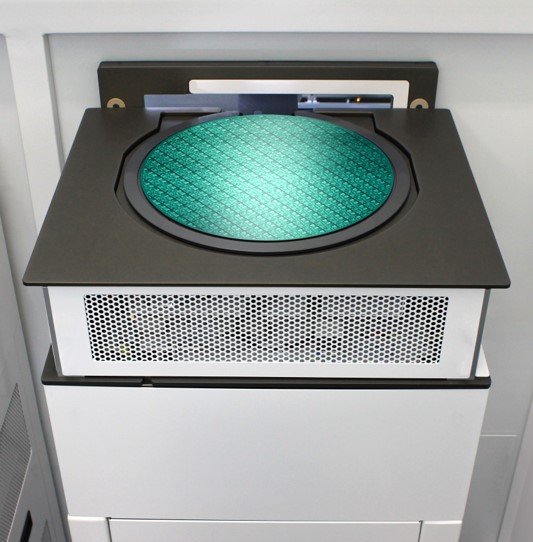
METRYX シリーズ製品
ラムリサーチの質量計測システムは、高度なプロセス監視と3次元デバイス構造の制御により、サブミリグラムレベルの計測能力を提供します。

OverViz
OverViz™は、プラズマ放電を忠実にモデリングするための産業用シミュレーションソフトウェア・プラットフォームです。
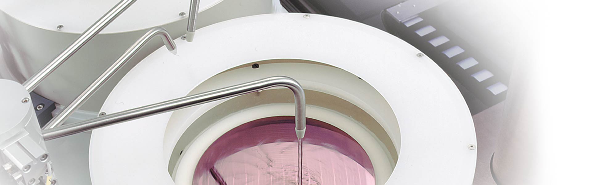
RELIANT クリーニング製品
ラムリサーチの RELIANTクリーニング製品は、スペシャルティ・テクノロジーのロードマップを実現し、ファブの生産寿命を延ばします。
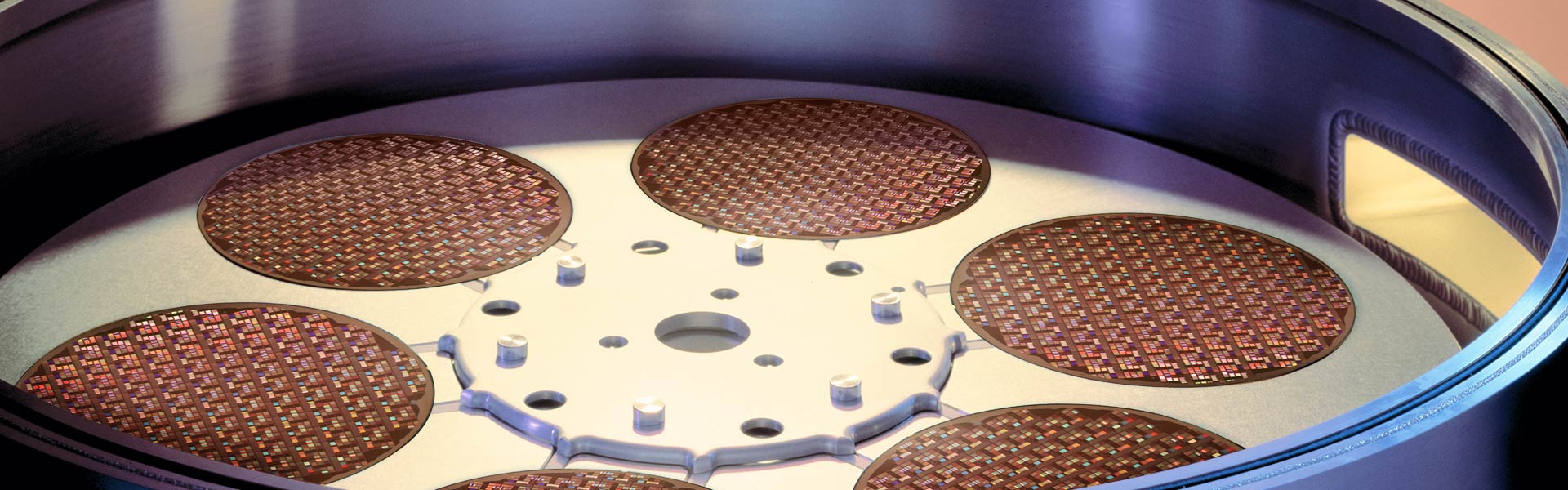
RELIANT成膜製品
RELIANT 成膜製品は、スペシャルティ・テクノロジーのロードマップを実現し、ファブの生産寿命を延ばします。
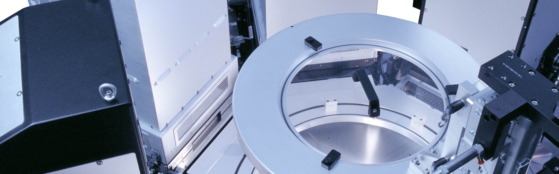
RELIANTエッチング製品
当社の RELIANT エッチング製品は、スペシャルティ・テクノロジーのロードマップを実現し、ファブの生産寿命を延ばします。
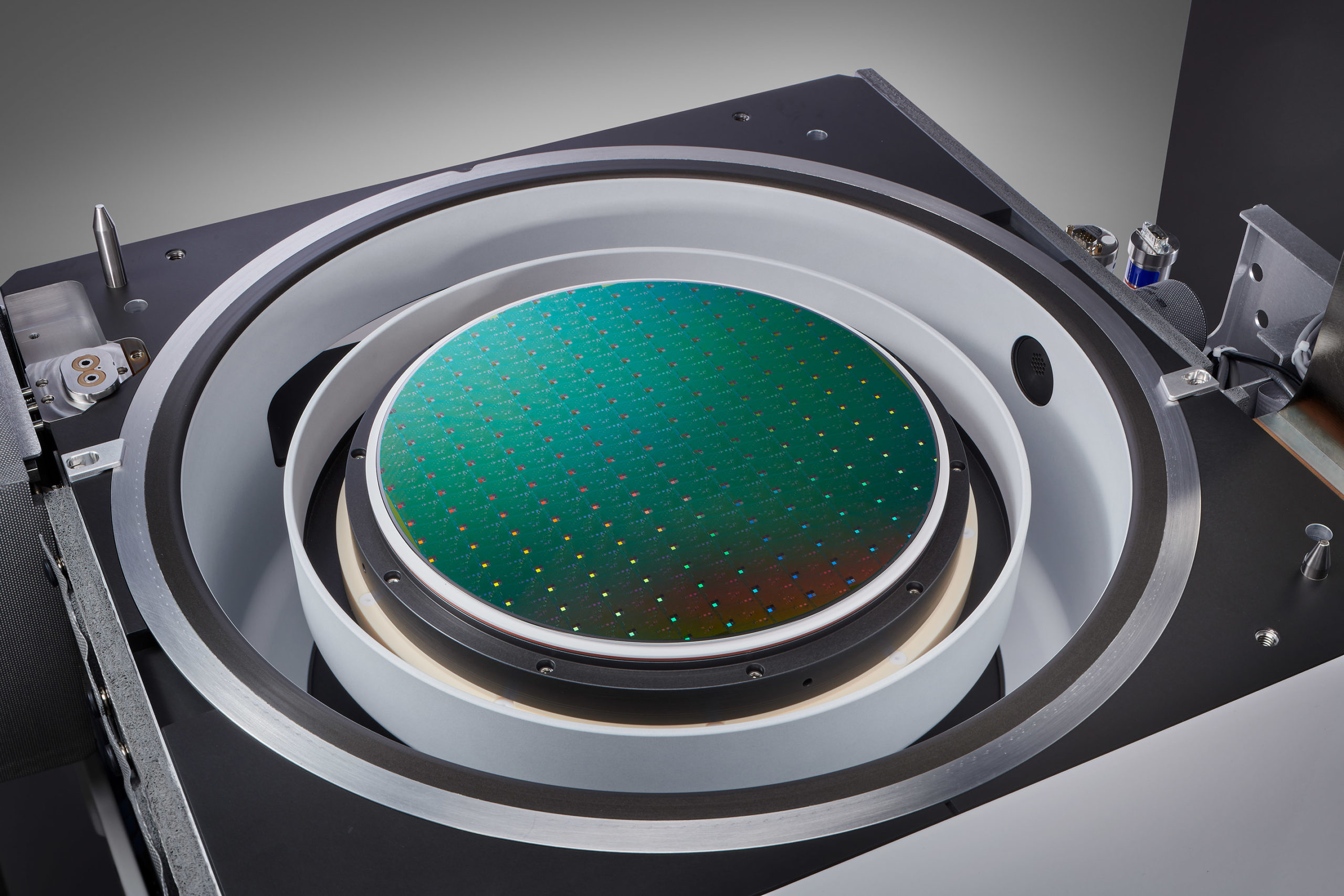
高選択エッチング製品群
画期的なポートフォリオにより、3D アーキテクチャ、先端ロジックおよびファウンドリ用途向けに、0.1nm スケールの精度と超高選択性で等方的材料除去を実現します。

SEMulator3D
半導体プロセスモデリング・プラットフォーム SEMulator3D® は広範囲にわたる技術開発環境を提供します。
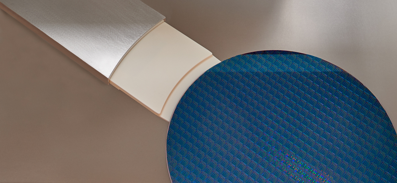
SENSE.I製品
私たちの最新エッチング装置のプラットフォームは、最高の生産性でプロセスパフォーマンスを提供するコンパクトで高密度のアーキテクチャで比類のないシステムインテリジェンスを実現します。
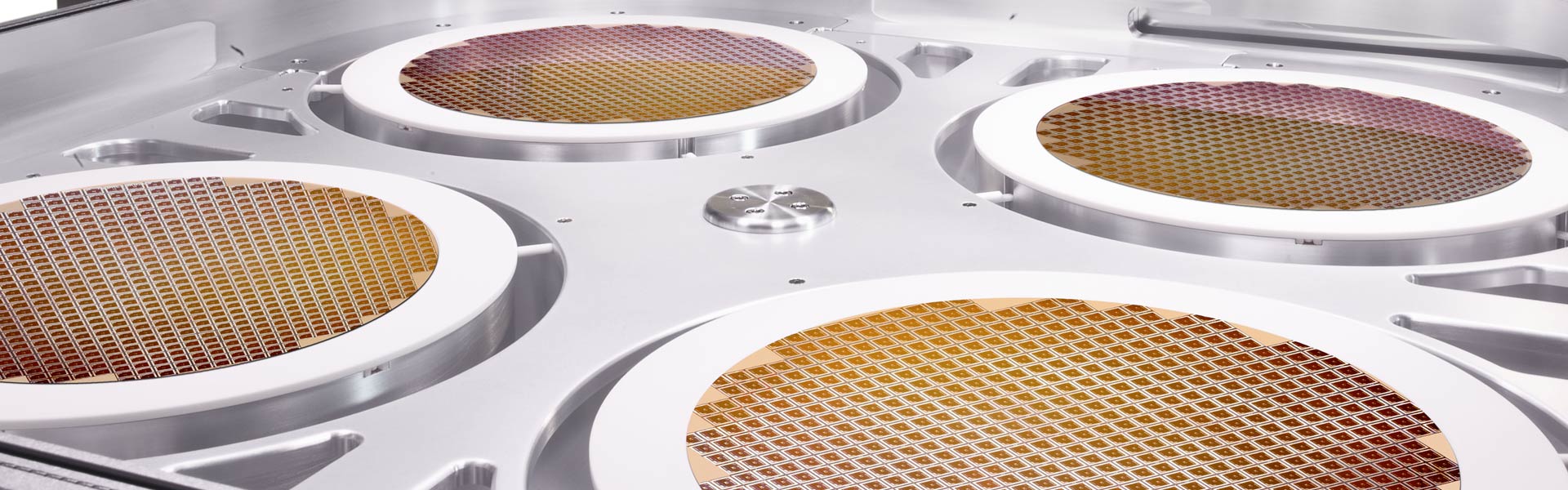
SOLA シリーズ製品
このシリーズ製品は、高度な膜アプリケーションの物理的特性を向上させる特殊な成膜後のトリートメント機能を提供します。
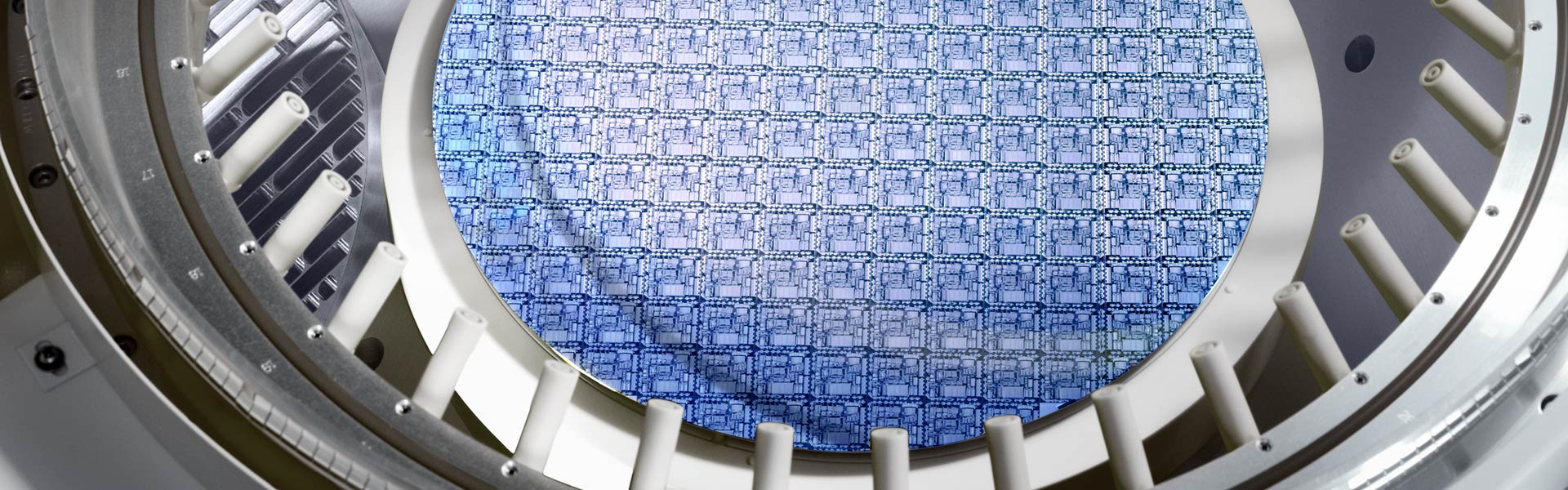
SPEED シリーズ製品
これらの酸化膜成膜製品は、業界最高のスループットと信頼性を備えた高アスペクト比スペースの完全なギャップフィル機能を提供します。
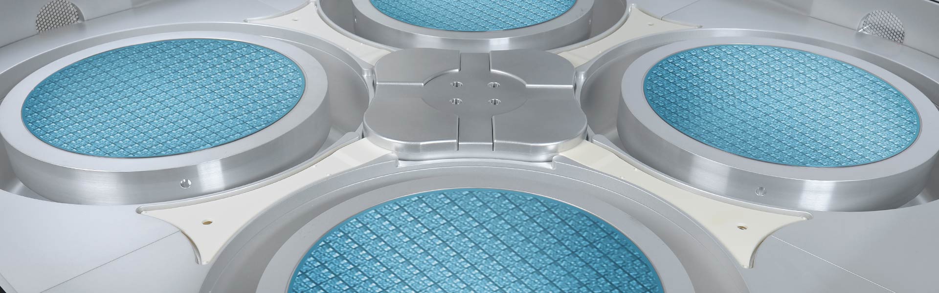
STRIKER シリーズ製品
高度なALD技術を活用することにより、これらの製品はナノスケールの機能を備えた高度なデバイスのクリティカルプロセスに対して優れた制御性能を実現する酸化膜を提供します。
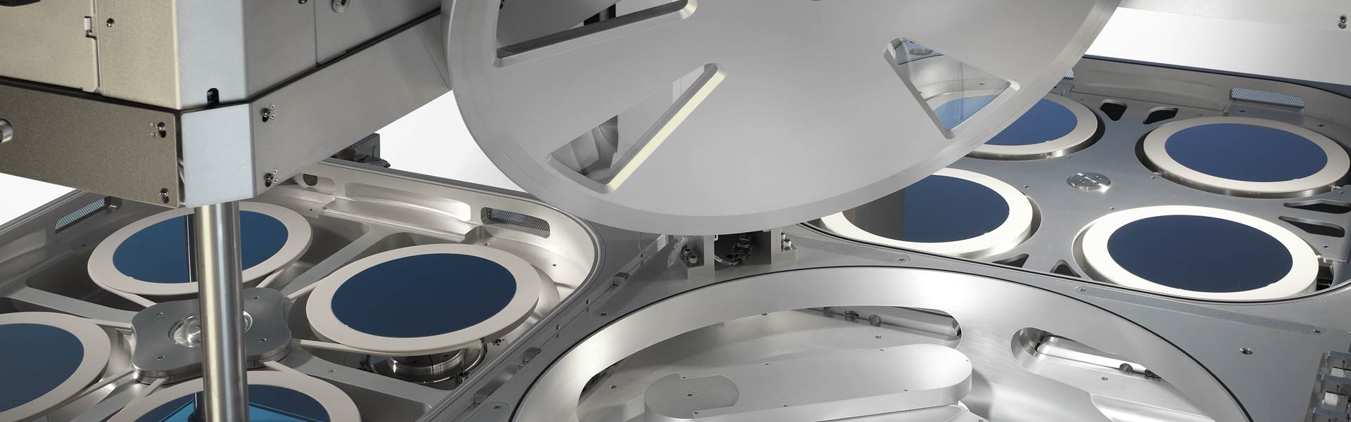
VECTOR シリーズ製品
ラムリサーチ社のPECVD製品ファミリーは、幅広いデバイスアプリケーションに対応した高い生産性の精密な酸化膜成膜を提供します。
Related Blog Posts
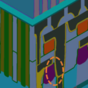
Understanding CFETs, a Next Generation Transistor Architecture
Computing power has experienced exponential growth over the last 70 years. This has largely been achieved through transistor scaling. Due to a continuous reduction in the size of transistors, engineers have been able to pack more and more of them onto a single chip[1]. This has led to faster, more powerful, and more energy-efficient devices. Improvements in fabrication processes and materials, along with better circuit design techniques, have enabled this scaling. As transistors have become smaller and more densely packed, we have started to reach limitations caused by the laws of physics.
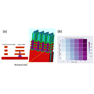
Improving Gate All Around (GAA) Transistor Performance using Virtual Process Window Exploration
As transistor sizes shrink, short channel effects make it more difficult for transistor gates to turn a transistor ON and OFF [1]. One method to overcome this problem is to move away from planar transistor architectures toward 3D devices. Gate-all-around (GAA) architectures are an example of this type of 3D device [2]. In a GAA transistor, the gate oxide surrounds the channel in all directions. A key process during the fabrication of GAA transistors involves the channel release step.