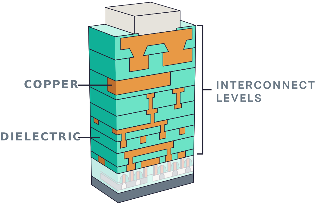
配線工程はチップ上の何10億個もの回路素子(トランジスタやコンデンサなど)を繋ぐために複雑な層間配線を形成する物です。チップ上の素子密度が高まるにつれ、全てを正しく繋ぐのに必要な配線層も増えるので、生産工程は難しくなります。現実問題として、微細化による寸法の縮小により、最先端のデバイスにおいては配線がチップの処理速度を遅くする要因になってきています。そのため、メタル接合の電気抵抗を低減する技術や、絶縁性能を高めるための新たな誘電体材料が必要になってきています。 最先端の高性能電子デバイスで採用される配線構造は極めて微細な構造で、しかも複雑な薄膜層を使います。そのため、柔軟性が高く、精密なプロセス能力が必要です。
ラムリサーチのソリューション
配線工程
ALTUS製品ファミリー
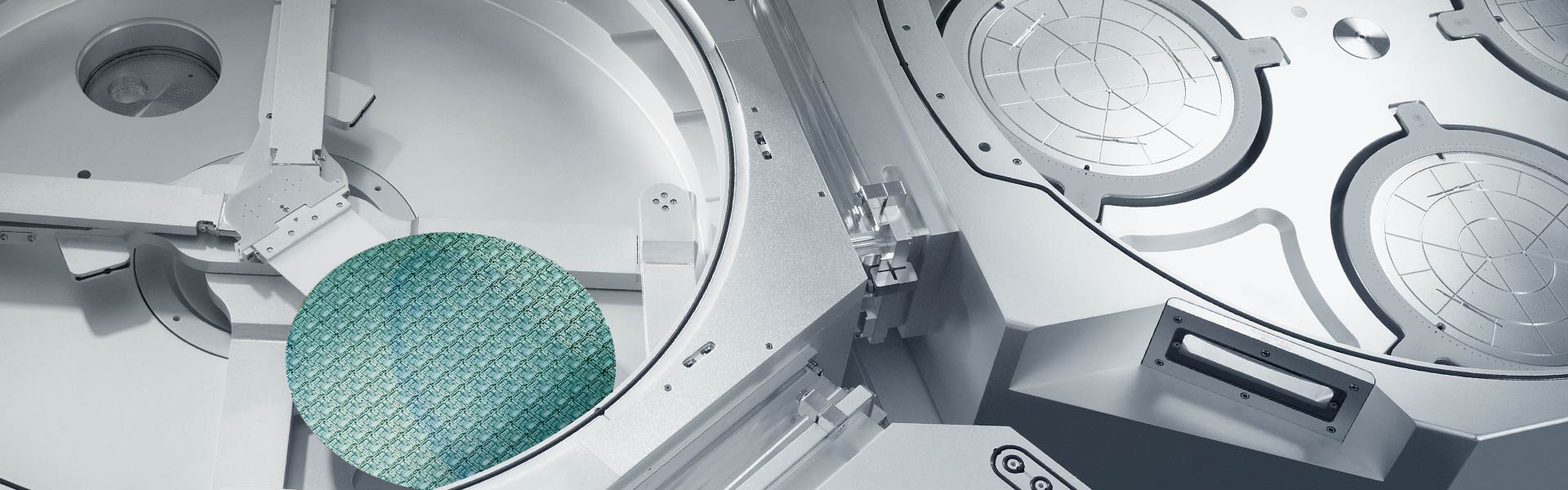
CVDとALD技術を組み合わせた市場をリードするこれらのシステムにより、先進的なタングステンメタライゼーション用途向けに高コンフォーマルな金属膜を成膜します。

CORONUSシリーズ製品
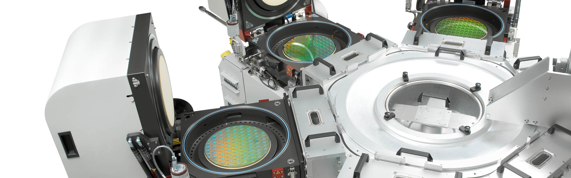
半導体製造工程全体の歩留まりを向上させるためにCoronus システムはウェハのベベルエッジに着目しました。半導体製造工程を通じてウェハエッジ部には残渣や残膜 やラフネスが蓄積します。これが剥がれ落ちて他の場所に付着すると欠陥となり、デバイス不良を引き起こす原因なります。Coronus エッチはベベルの残渣を除去し、Coronus デポジションはベベルをダメージから保護する製品です。
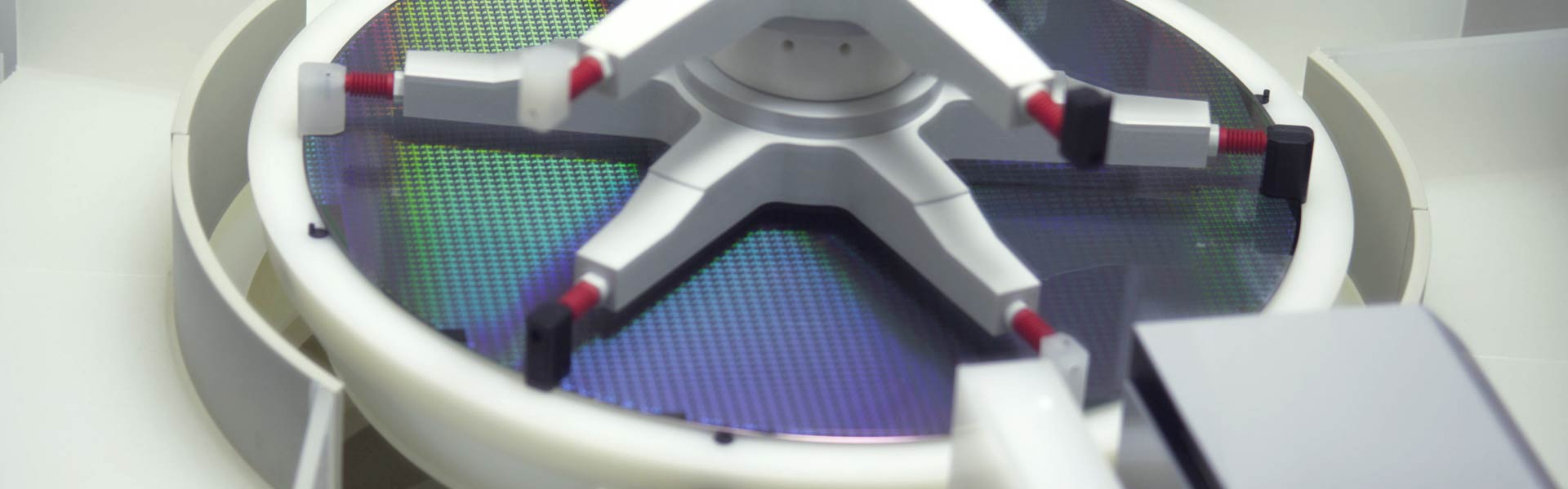
DV-PRIME & DA VINCI シリーズ
これらの製品は製造工程全体にわたる複数のウェハクリーニングステップにおいて求められる高い生産性と柔軟性を実現するプロセスを提供します。
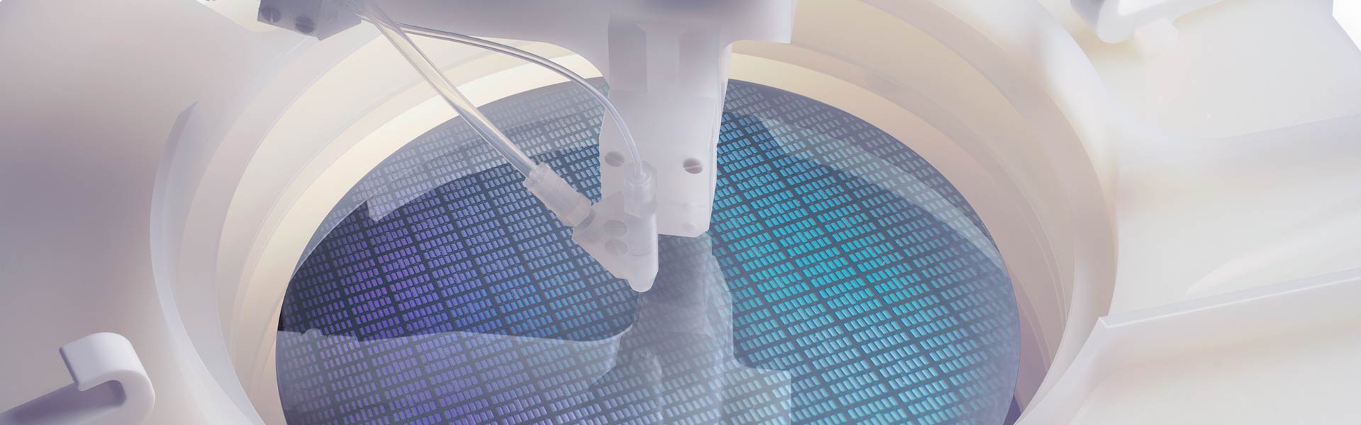
EOS シリーズ製品
ラムリサーチの先進的なウェットクリーン製品は、厳しい要求条件の用途に対して高スループットで不良率が低いウェハ生産を可能にします。

Fabtex™ Yield Optimizer
Fabtex™ Yield Optimizer is a cutting-edge software platform designed to help semiconductor foundries accelerate yield ramp and improve high-volume manufacturing performance.
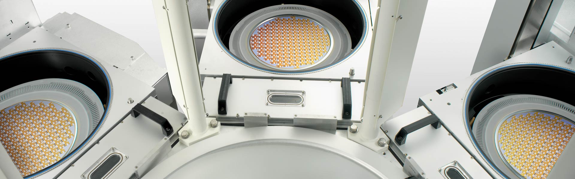
FLEX シリーズ製品
ラムリサーチの酸化膜エッチシステムは、先進のデバイスに求められる複雑な構造を備えた幅広いアプリケーションに配慮した機能を提供します。
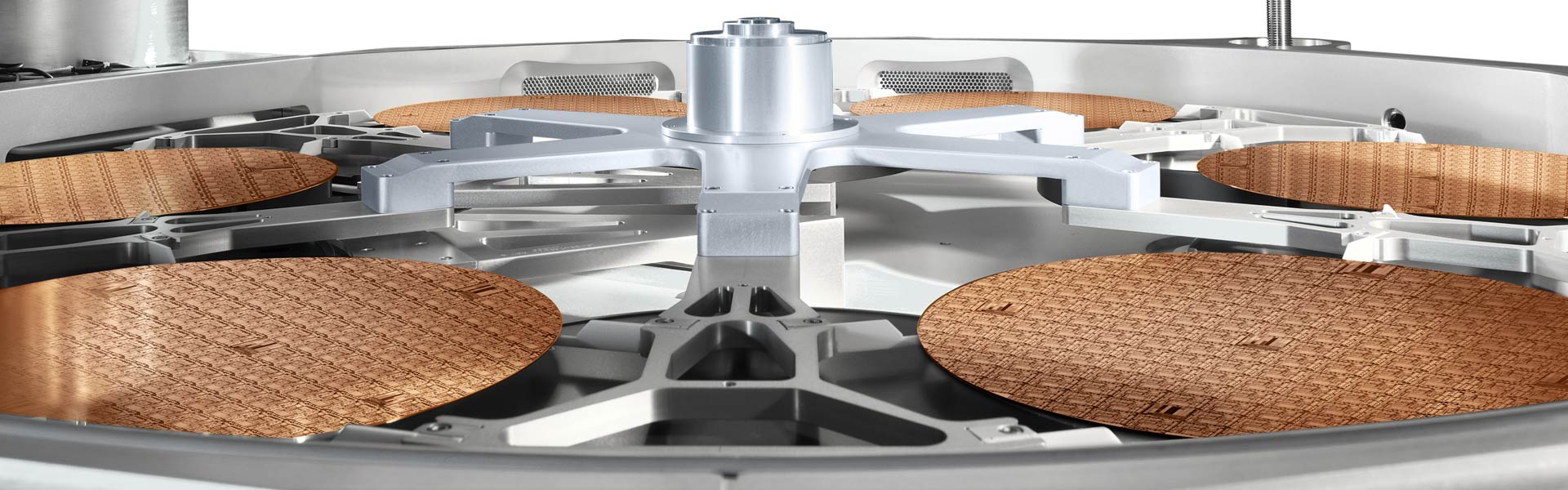
GAMMAシリーズ製品
これらの製品は、各種のクリティカルなフォトレジスト ストリップ アプリケーションに対応した高いプロセス柔軟性を提供します。
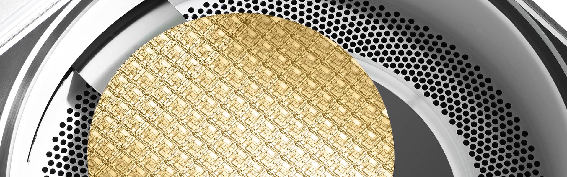
KIYO シリーズ製品
業界をリードするコンダクターエッチング製品は、クリティカルなデバイス機能に必要な高精度と高い生産性での制御を実現します。
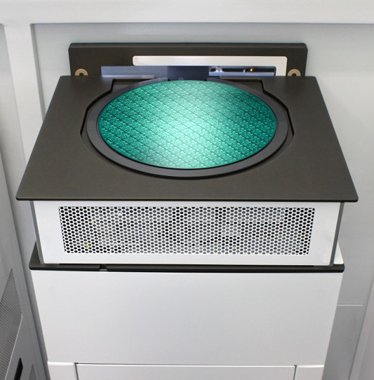
METRYX シリーズ製品
ラムリサーチの質量計測システムは、高度なプロセス監視と3次元デバイス構造の制御により、サブミリグラムレベルの計測能力を提供します。

OverViz
OverViz™は、プラズマ放電を忠実にモデリングするための産業用シミュレーションソフトウェア・プラットフォームです。
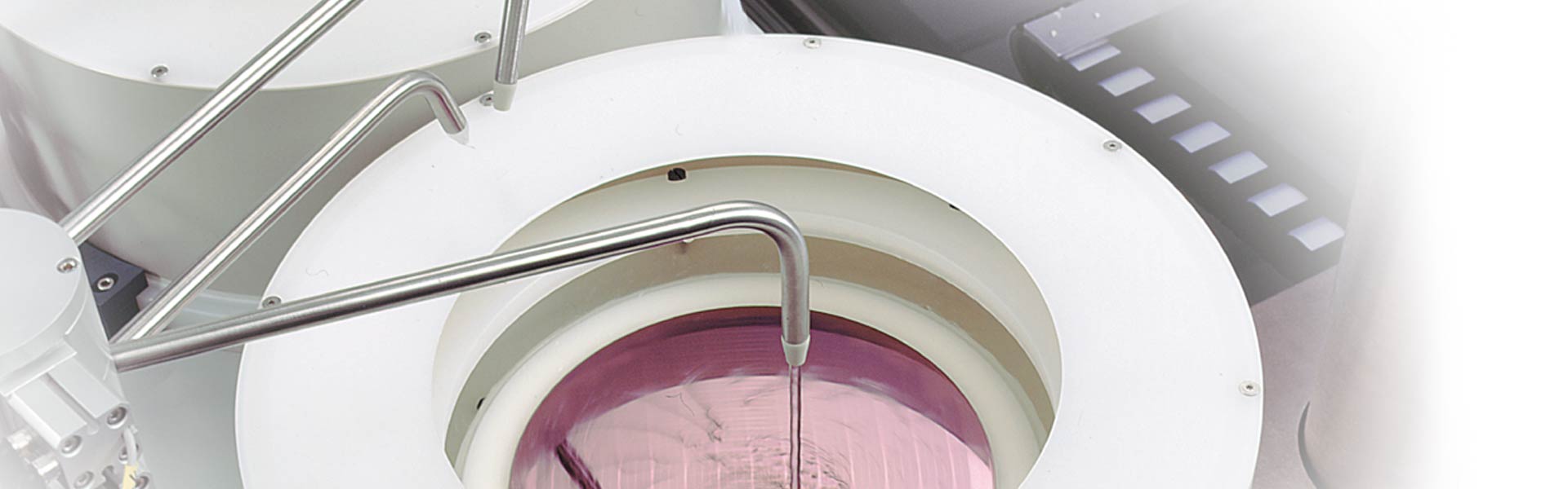
RELIANT クリーニング製品
ラムリサーチの RELIANTクリーニング製品は、スペシャルティ・テクノロジーのロードマップを実現し、ファブの生産寿命を延ばします。
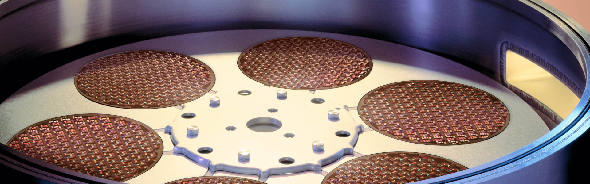
RELIANT成膜製品
RELIANT 成膜製品は、スペシャルティ・テクノロジーのロードマップを実現し、ファブの生産寿命を延ばします。
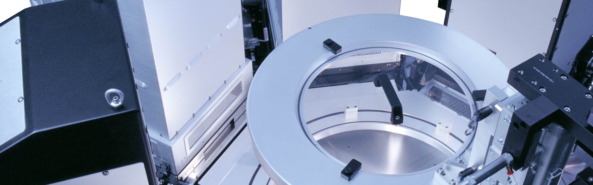
RELIANTエッチング製品
当社の RELIANT エッチング製品は、スペシャルティ・テクノロジーのロードマップを実現し、ファブの生産寿命を延ばします。
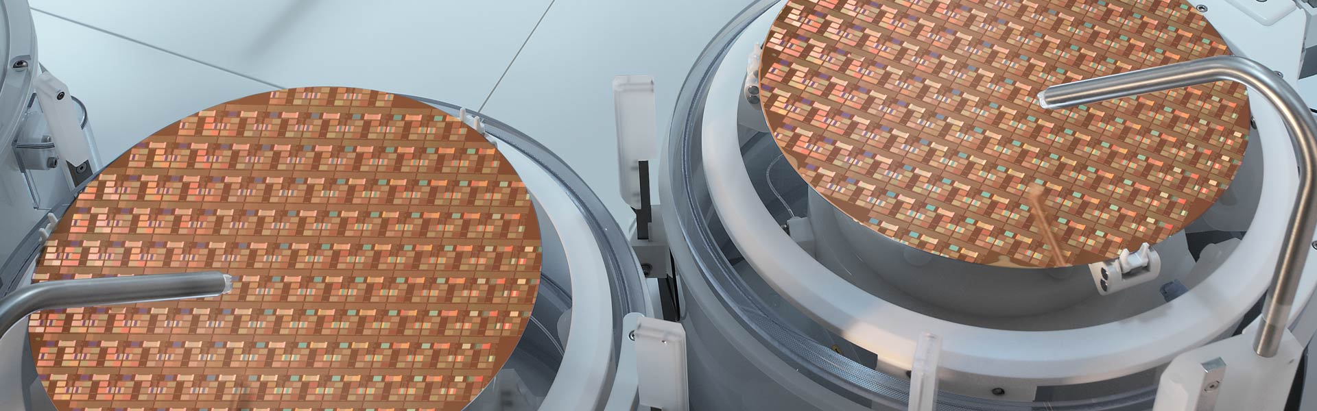
SABRE シリーズ製品
実績のあるElectrofill技術により、これらの高生産性システムは高度なパッケージングアプリケーションを開発するための高品質な金属膜を提供します。
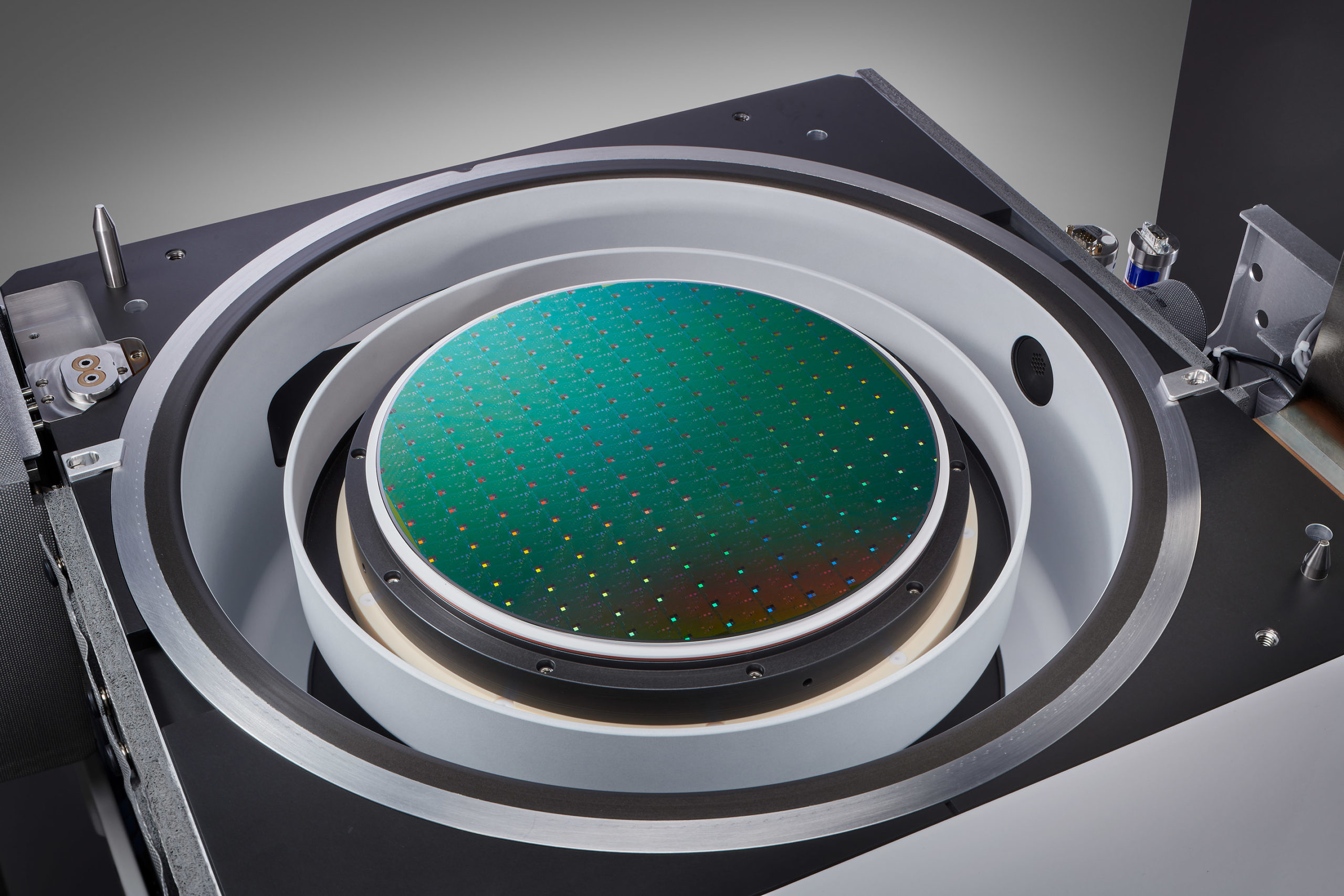
高選択エッチング製品群
画期的なポートフォリオにより、3D アーキテクチャ、先端ロジックおよびファウンドリ用途向けに、0.1nm スケールの精度と超高選択性で等方的材料除去を実現します。
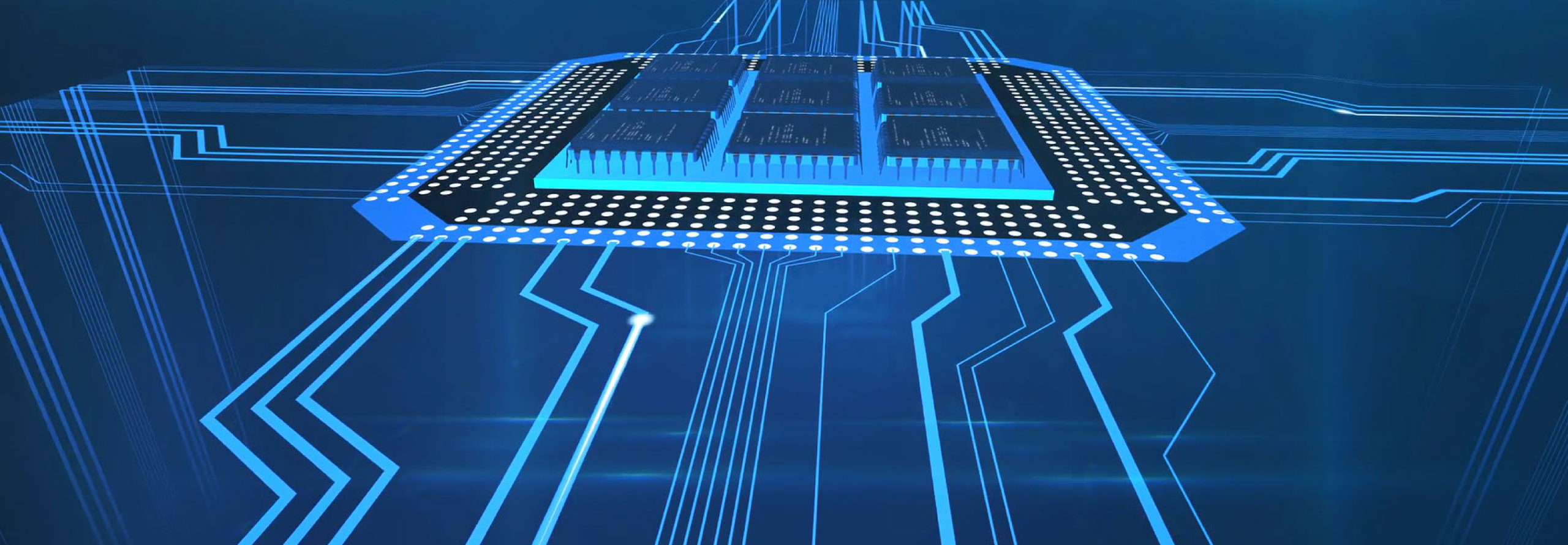
SEMulator3D
半導体プロセスモデリング・プラットフォーム SEMulator3D® は広範囲にわたる技術開発環境を提供します。
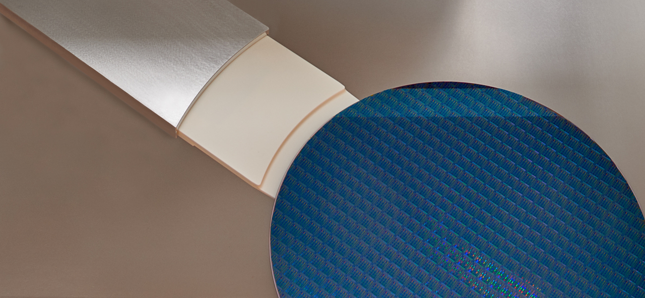
SENSE.I製品
私たちの最新エッチング装置のプラットフォームは、最高の生産性でプロセスパフォーマンスを提供するコンパクトで高密度のアーキテクチャで比類のないシステムインテリジェンスを実現します。
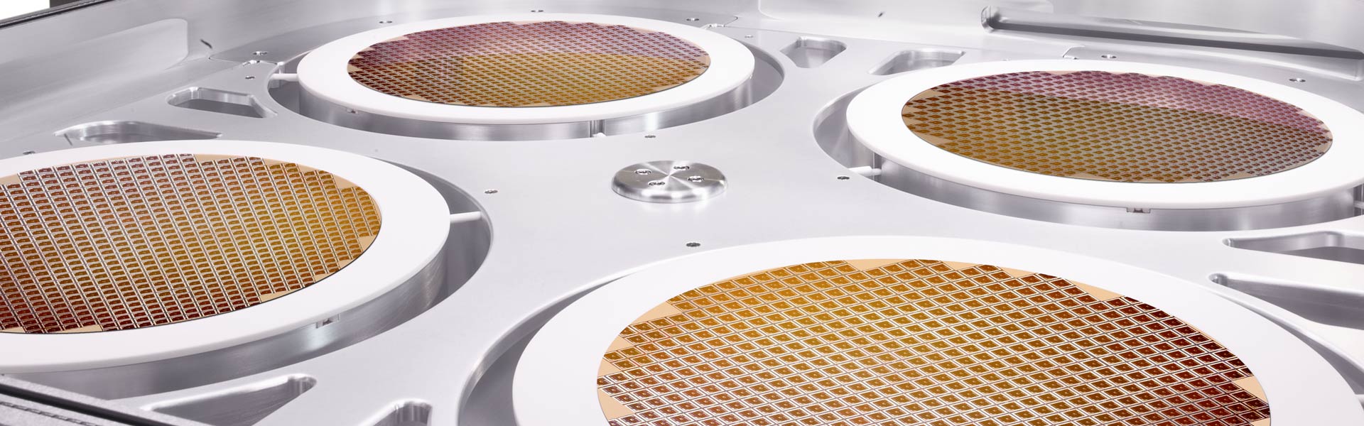
SOLA シリーズ製品
このシリーズ製品は、高度な膜アプリケーションの物理的特性を向上させる特殊な成膜後のトリートメント機能を提供します。
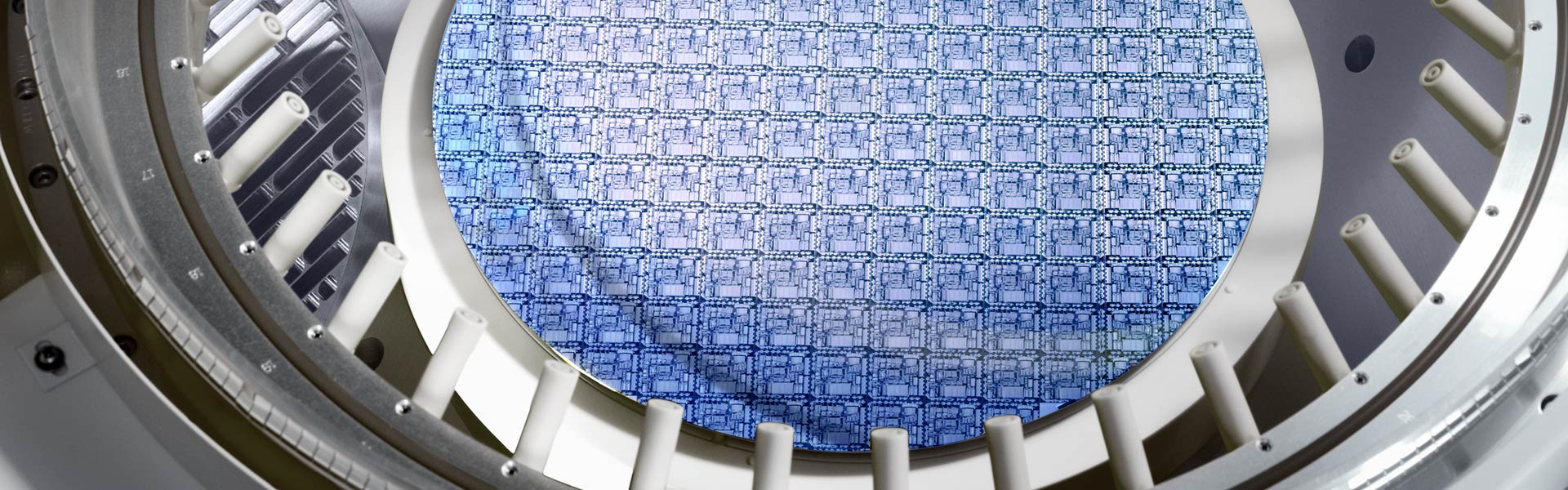
SPEED シリーズ製品
これらの酸化膜成膜製品は、業界最高のスループットと信頼性を備えた高アスペクト比スペースの完全なギャップフィル機能を提供します。
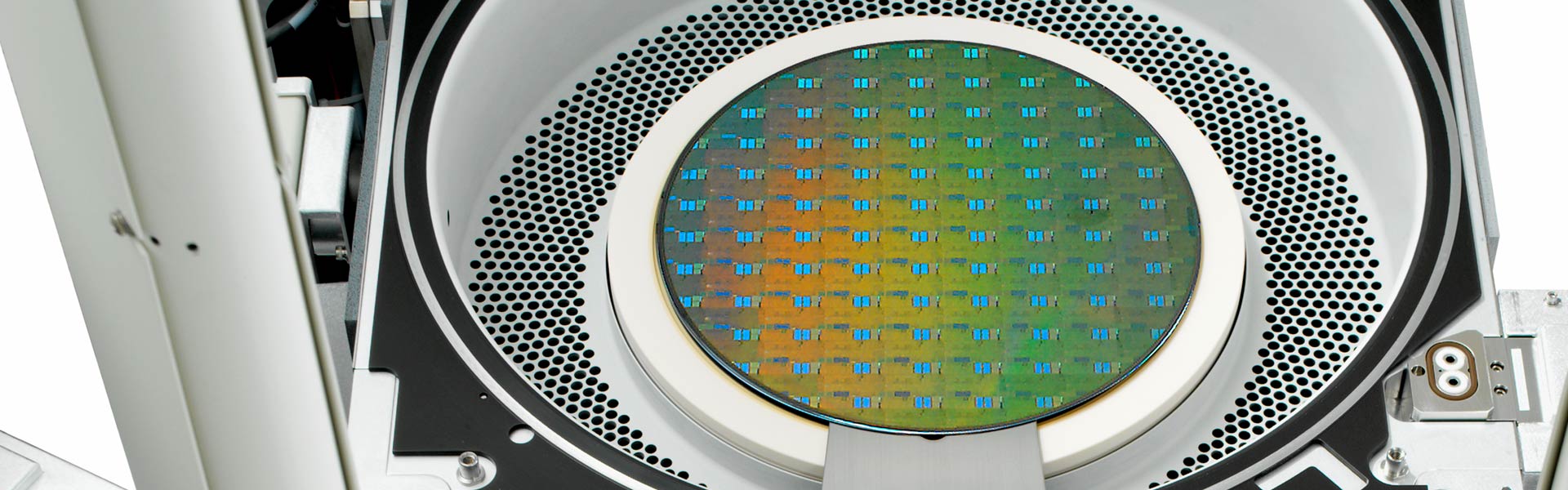
Syndion製品ファミリー
ディープエッチング用途では、高アスペクト比の重要な形状に必要な卓越したウェーハ全体にわたる均一性制御を提供します。
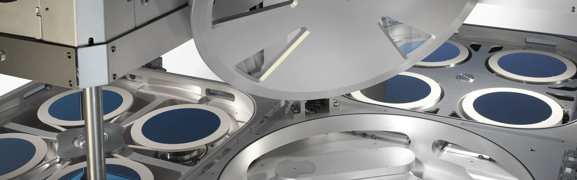
VECTOR シリーズ製品
ラムリサーチ社のPECVD製品ファミリーは、幅広いデバイスアプリケーションに対応した高い生産性の精密な酸化膜成膜を提供します。
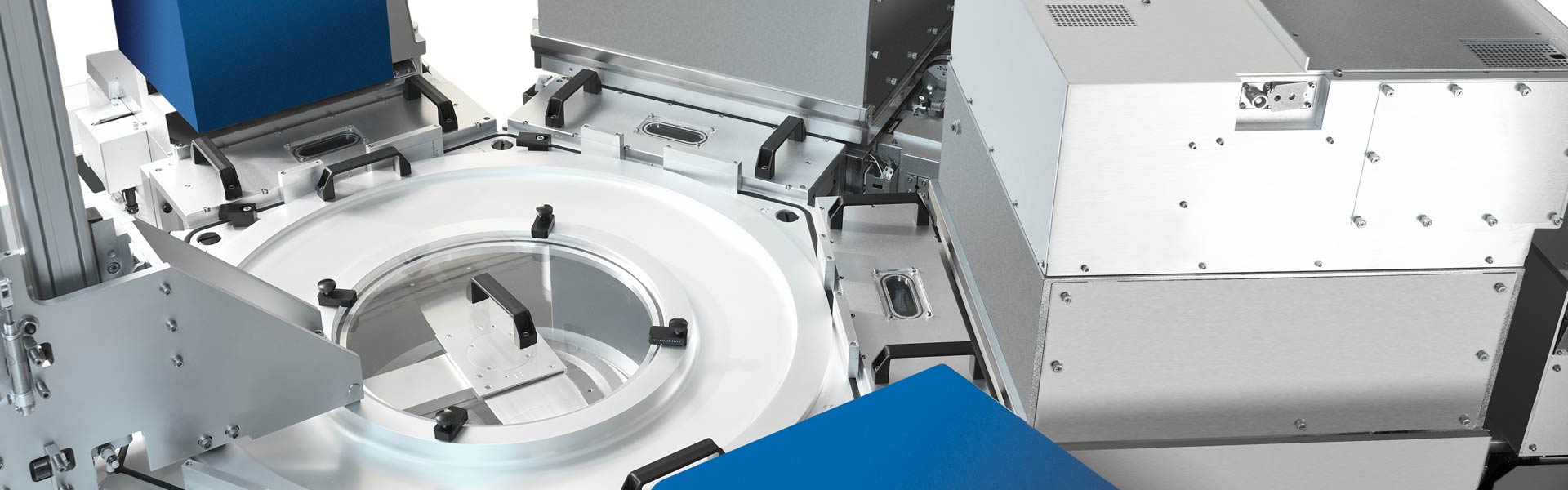
VERSYS METAL シリーズ製品
これらのメタルエッチング製品は、電気配線およびメタルハードマスク用途向けに高い生産性を備えたプロセス制御を提供します。
Related Blog Posts

Will Moly Replace Tungsten in Semiconductors?
To keep pace with Moore's Law and enable greater interconnect scaling, the semiconductor ecosystem is continually experimenting with variations of materials. Tungsten has been the interconnect metal of choice for nearly a quarter century in NAND, DRAM, and logic/foundry middle-of-line applications. But scaling requirements are now pushing the boundaries of what is possible with tungsten. A variety of metals are being considered, but one — molybdenum — is an especially promising candidate. At the atomic dimensions required for advanced chipmaking, moly is emerging as the most suitable material to replace tungsten, creating a major inflection in the industry.
A Deposition and Etch Technique to Lower Resistance of Semiconductor Metal Lines
Cu’s resistivity depends on its crystal structure, void volume, grain boundaries and material interface mismatch, which becomes more significant at smaller scales. The formation of Cu wires is traditionally done by etching a trench pattern in low-k silicon dioxide using a trench etch process, and subsequently filling the trench with Cu via a damascene flow. Unfortunately, this method produces multi-crystalline structures with significant grain boundaries and voids, which increases the Cu wire resistance. A highly resistive TaN liner material is also utilized in this process to prevent Cu diffusion during the damascene annealing process.