
電子データを保存する半導体部品であるメモリ・セルには、短期の揮発性(DRAMなど)と長期の不揮発性(フラッシュなど)のストレージ・タイプがあります。 DRAMは「作業」メモリ(アクティブメモリ)の代表です。フラッシュメモリは大容量のデータをコンパクトに保存するために使用されます。
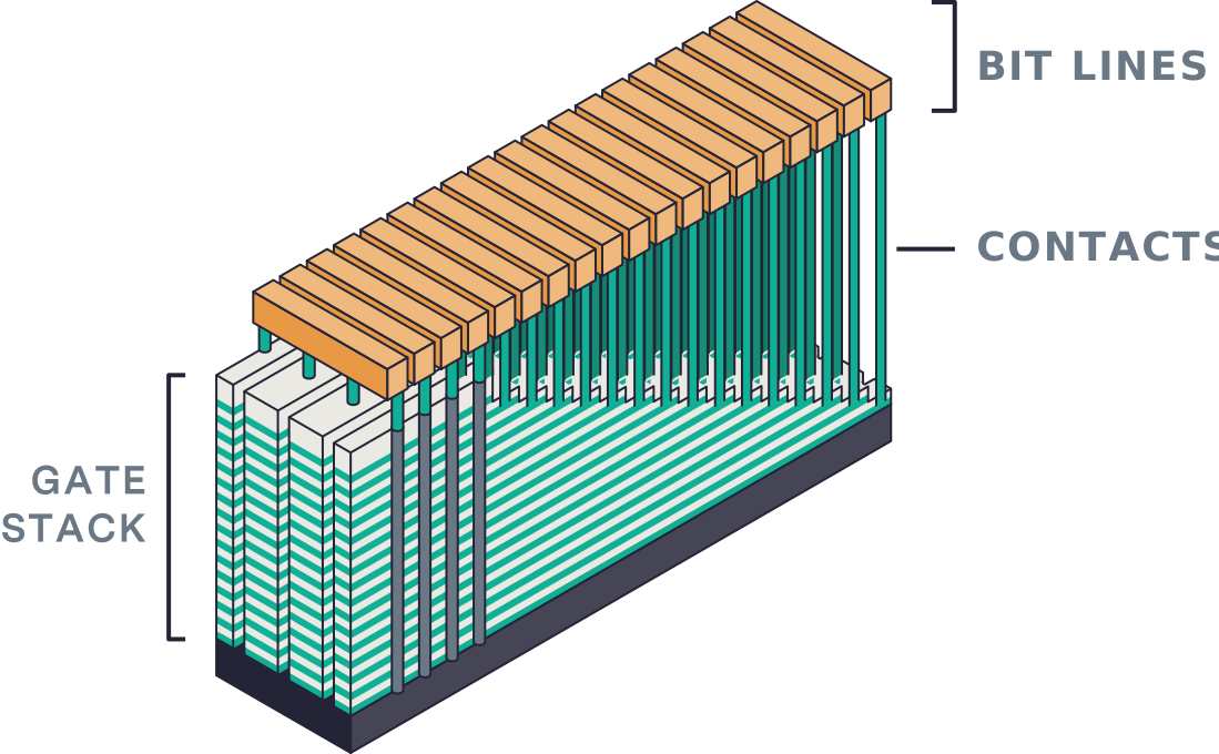
デバイス密度を高めてストレージ容量を増やすために、DRAM機能は縮小を続け、NANDフラッシュは3Dアーキテクチャに移行しているが、さらなる処理上の課題が生じています。 例えば、3D NANDの多数の層はストレスに弱く、高アスペクト比のチャネルに欠陥があると、電気的なショートや干渉が発生する可能性があります。 アクティブ・クラスとストレージ・クラスのギャップを埋める新しいタイプのメモリーの生産も、新しい、加工が難しい材料を使用するため困難となっています。 その結果、卓越した工程管理、柔軟性、生産性が求められます。
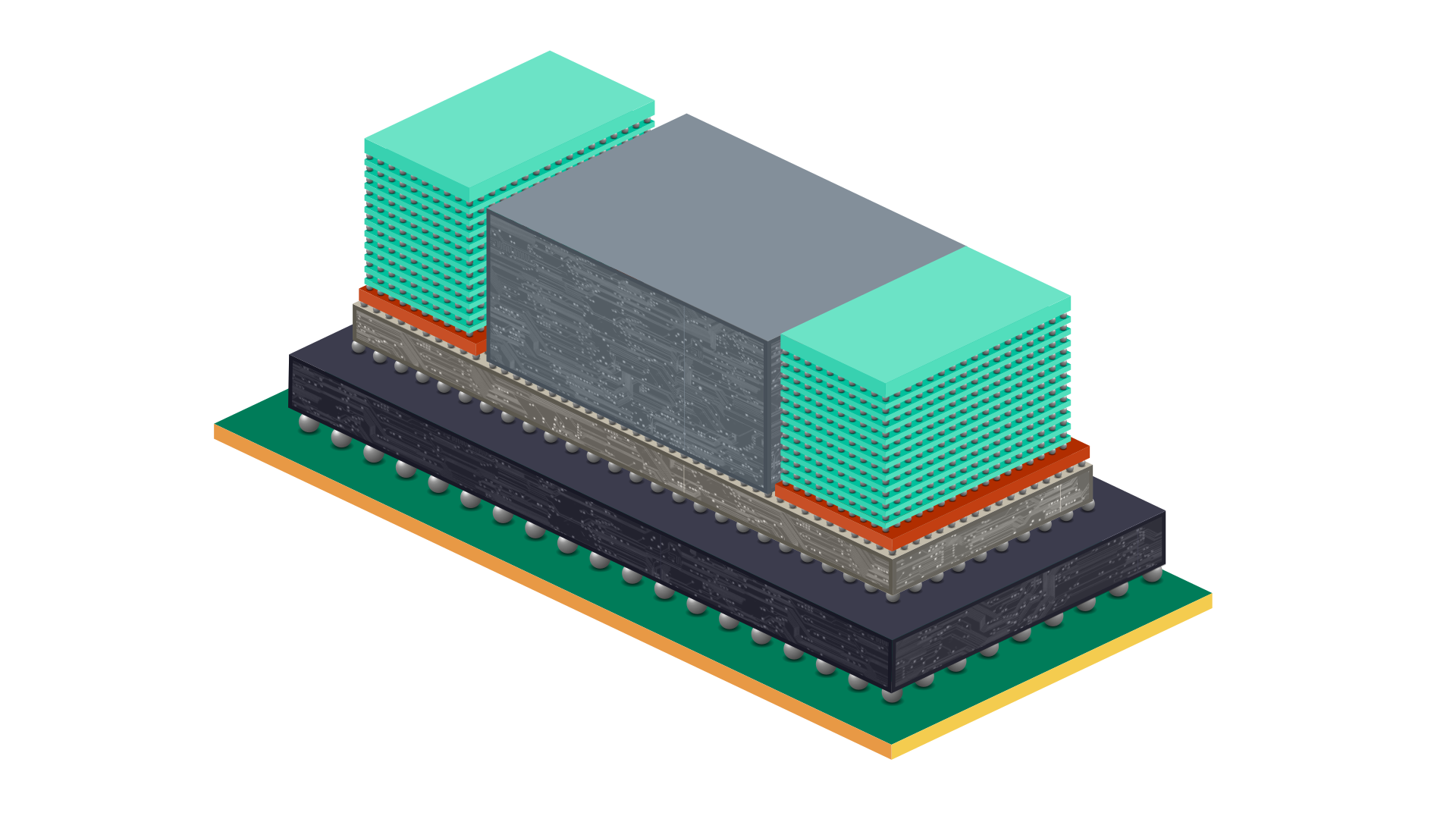
技術革新をリードすることで、Lamは自社のメモリ・ソリューションが進化するテクノロジーの要求に確実に応えられるようにしています。 AI、VR、AR、電気自動車の需要の急増に対応するため、我々が革新を進めている分野の1つに、高帯域幅メモリー(HBM)技術があります。 HBMは、3Dスタッキングと最先端のパッケージングにより、高性能コンピューティングの未来を具現化し、比類ない性能と効率を約束します。
ハイブリッドボンディングのオンウェハ性能や歩留まり管理など、高度なメモリ製造の複雑な課題に直面する中、マイクロバンプやシリコン貫通電極(TSV)に関する当社の専門知識により、卓越したプロセス制御と生産性を提供することができます。
Lamのソリューション
高度なメモリ
ALTUS製品ファミリー
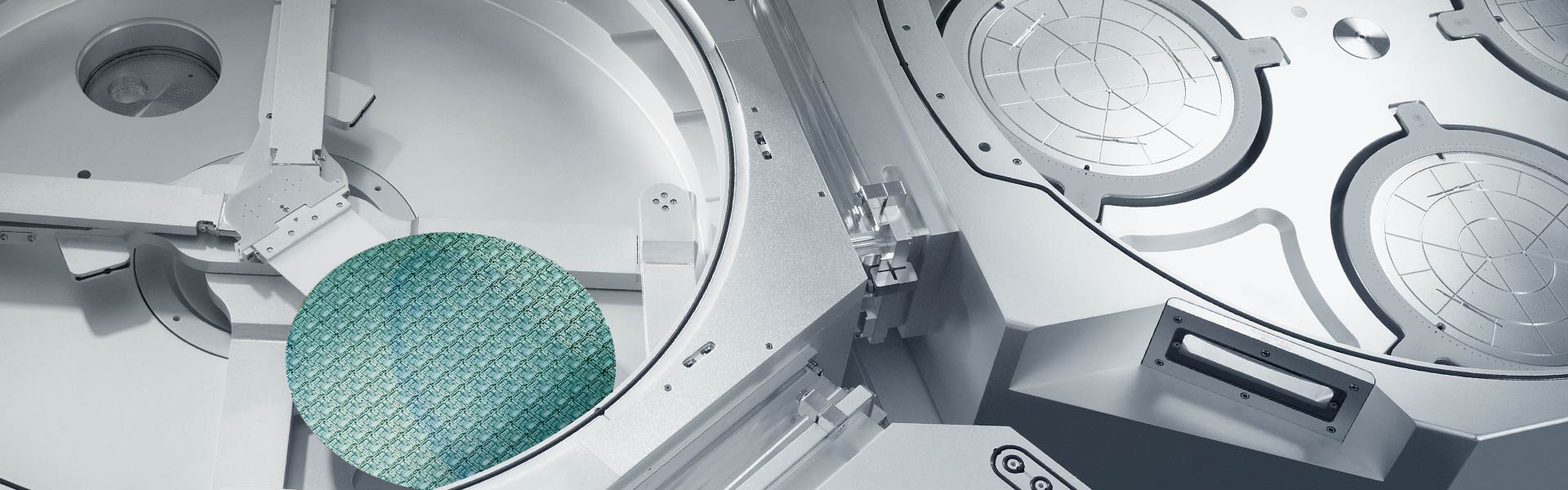
CVDとALD技術を組み合わせた市場をリードするこれらのシステムにより、先進的なタングステンメタライゼーション用途向けに高コンフォーマルな金属膜を成膜します。

CORONUSシリーズ製品
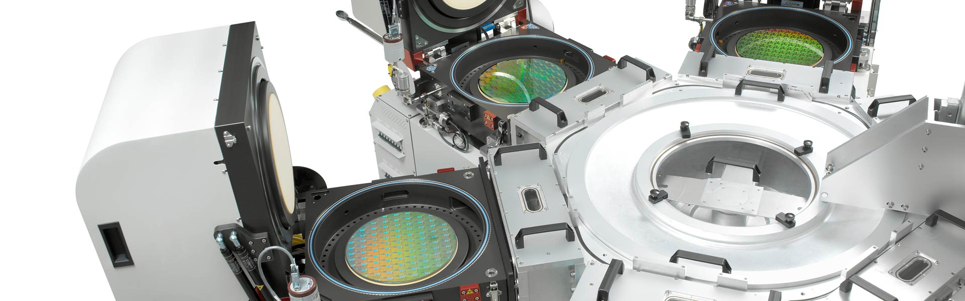
半導体製造工程全体の歩留まりを向上させるためにCoronus システムはウェハのベベルエッジに着目しました。半導体製造工程を通じてウェハエッジ部には残渣や残膜 やラフネスが蓄積します。これが剥がれ落ちて他の場所に付着すると欠陥となり、デバイス不良を引き起こす原因なります。Coronus エッチはベベルの残渣を除去し、Coronus デポジションはベベルをダメージから保護する製品です。
EOS シリーズ製品
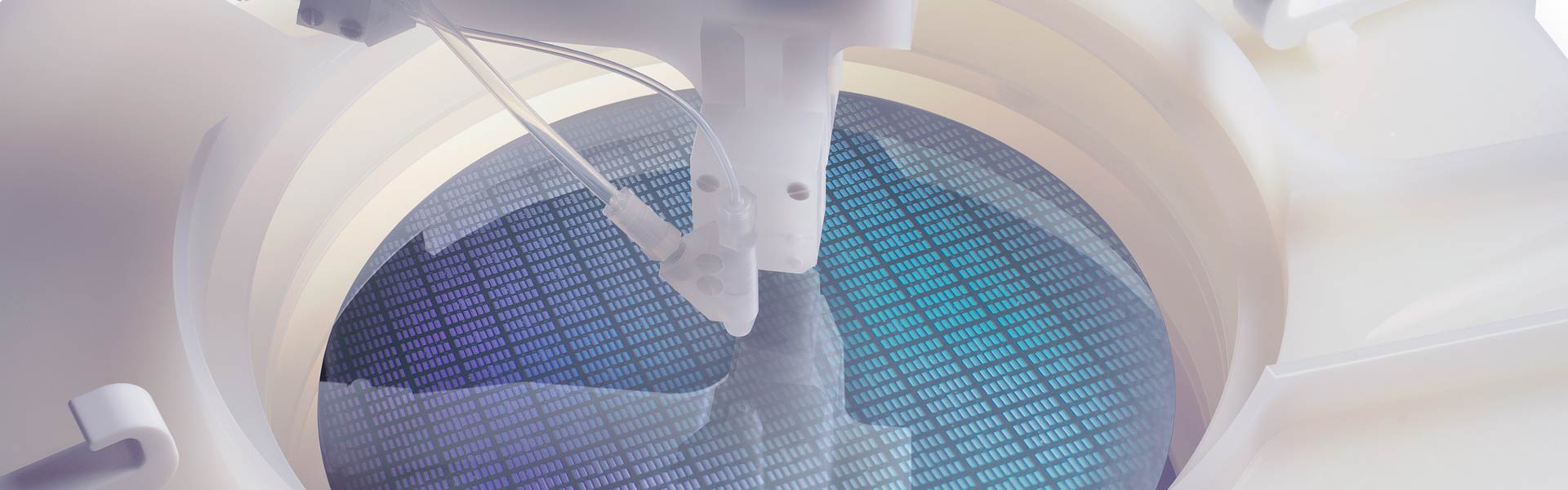
ラムリサーチの先進的なウェットクリーン製品は、厳しい要求条件の用途に対して高スループットで不良率が低いウェハ生産を可能にします。

Fabtex™ Yield Optimizer
Fabtex™ Yield Optimizer is a cutting-edge software platform designed to help semiconductor foundries accelerate yield ramp and improve high-volume manufacturing performance.
FLEX シリーズ製品
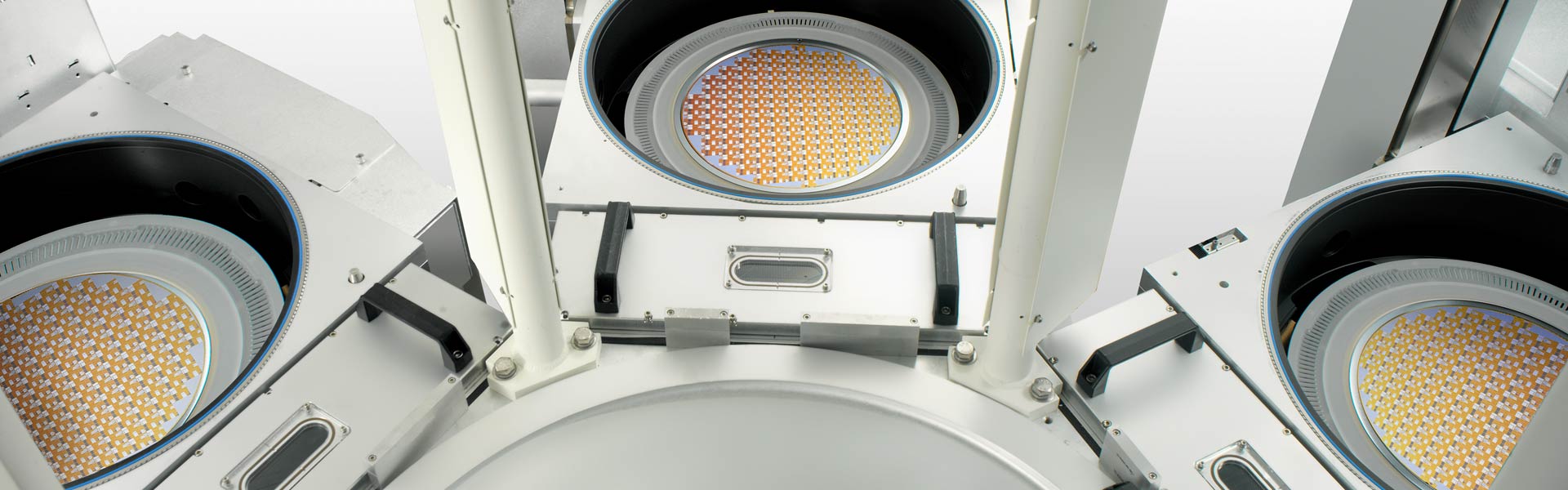
ラムリサーチの酸化膜エッチシステムは、先進のデバイスに求められる複雑な構造を備えた幅広いアプリケーションに配慮した機能を提供します。
GAMMAシリーズ製品
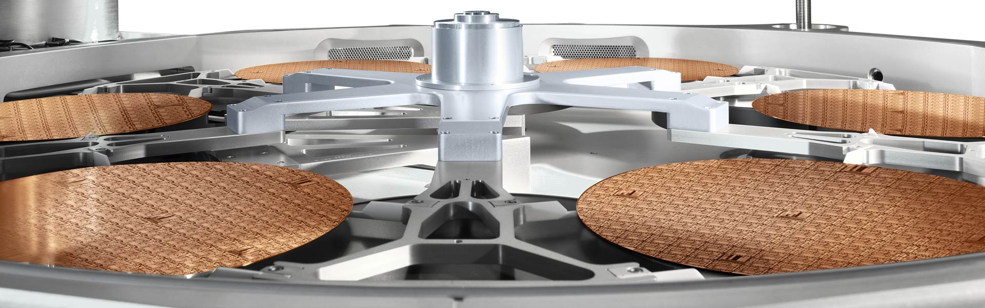
これらの製品は、各種のクリティカルなフォトレジスト ストリップ アプリケーションに対応した高いプロセス柔軟性を提供します。
カリスト製品シリーズ
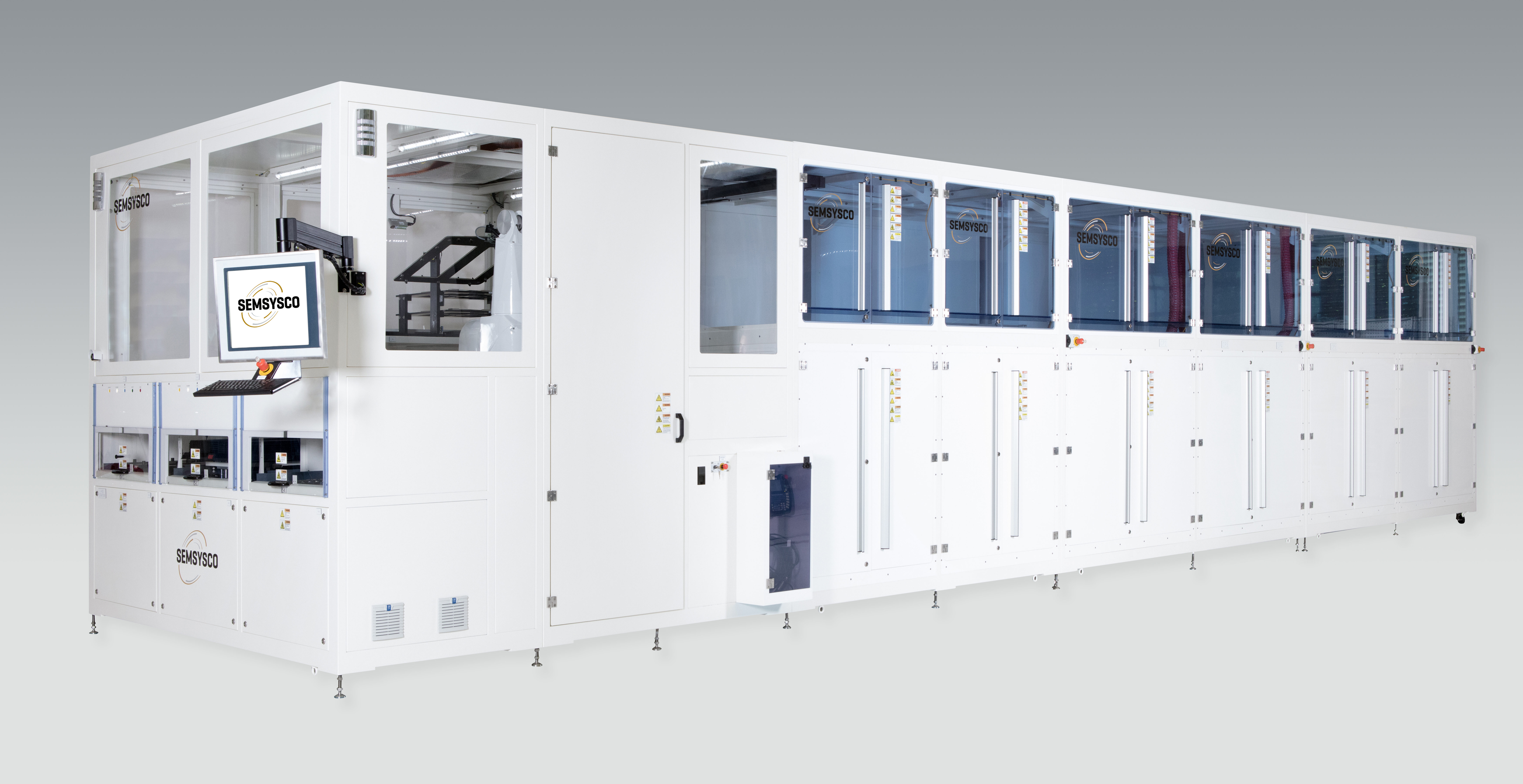
半導体業界のニーズに合わせた、300×300mmからGen5.1(1100x1300mm)までの基材をウェット処理するための先進的な縦型加工プラットフォーム。
KIYO シリーズ製品
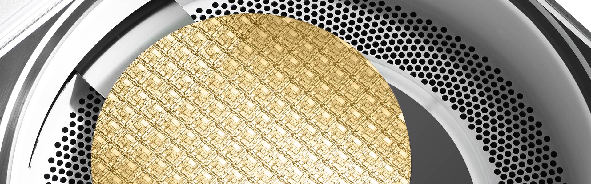
業界をリードするコンダクターエッチング製品は、クリティカルなデバイス機能に必要な高精度と高い生産性での制御を実現します。
METRYX シリーズ製品
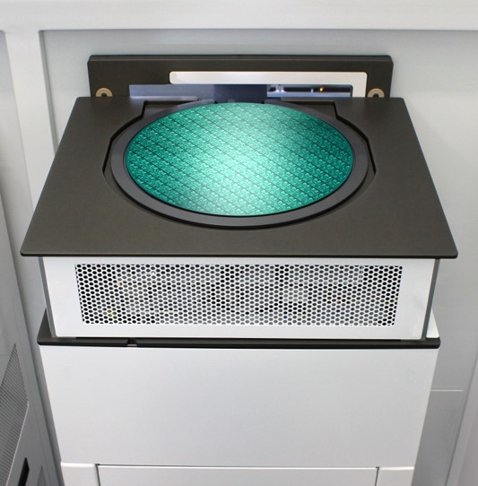
ラムリサーチの質量計測システムは、高度なプロセス監視と3次元デバイス構造の制御により、サブミリグラムレベルの計測能力を提供します。

OverViz
OverViz™は、プラズマ放電を忠実にモデリングするための産業用シミュレーションソフトウェア・プラットフォームです。
フェニックス製品シリーズ
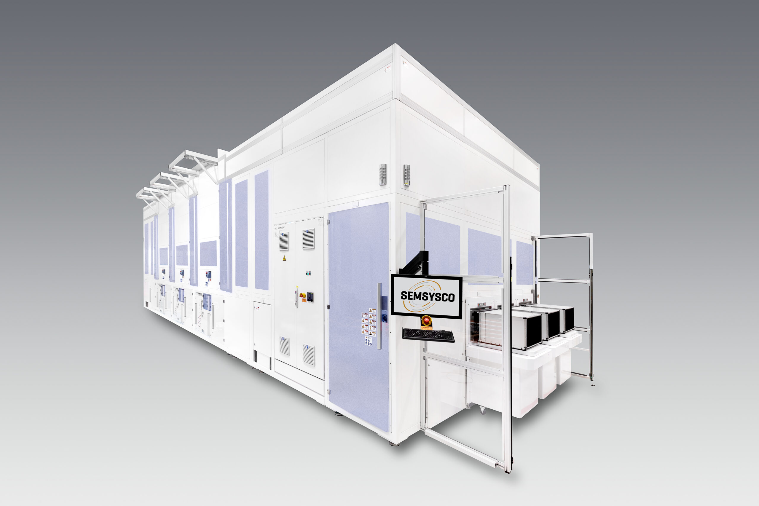
フェニックスは510x515mm 基板用の全自動大量パネル加工を提供します。
RELIANT成膜製品
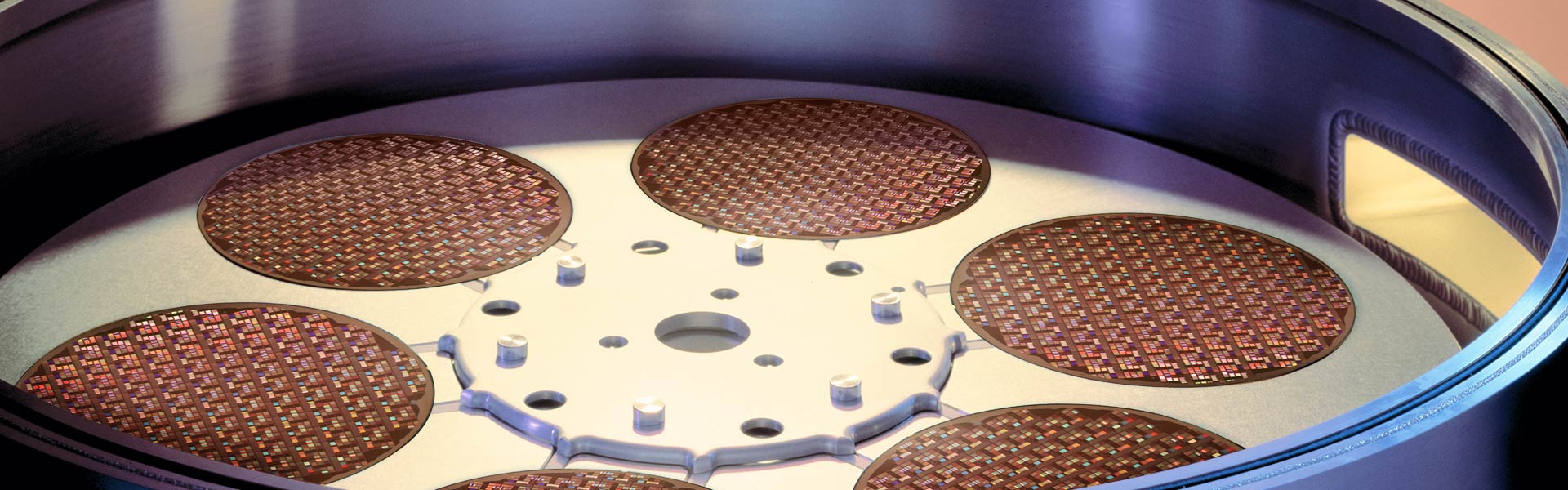
RELIANT 成膜製品は、スペシャルティ・テクノロジーのロードマップを実現し、ファブの生産寿命を延ばします。
RELIANTエッチング製品
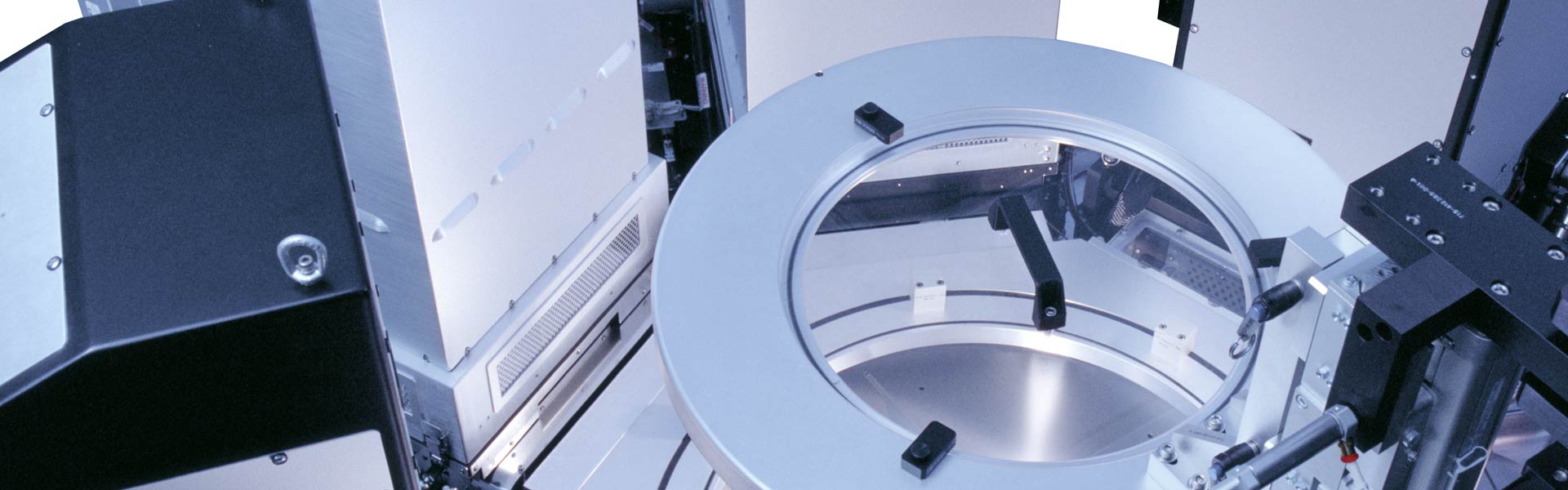
当社の RELIANT エッチング製品は、スペシャルティ・テクノロジーのロードマップを実現し、ファブの生産寿命を延ばします。
SABRE シリーズ製品
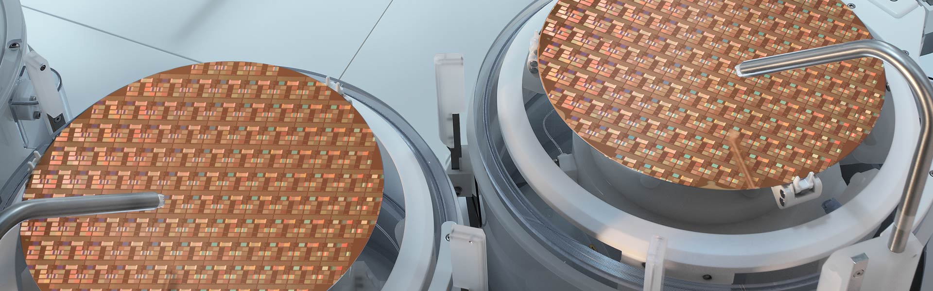
実績のあるElectrofill技術により、これらの高生産性システムは高度なパッケージングアプリケーションを開発するための高品質な金属膜を提供します。
高選択エッチング製品群
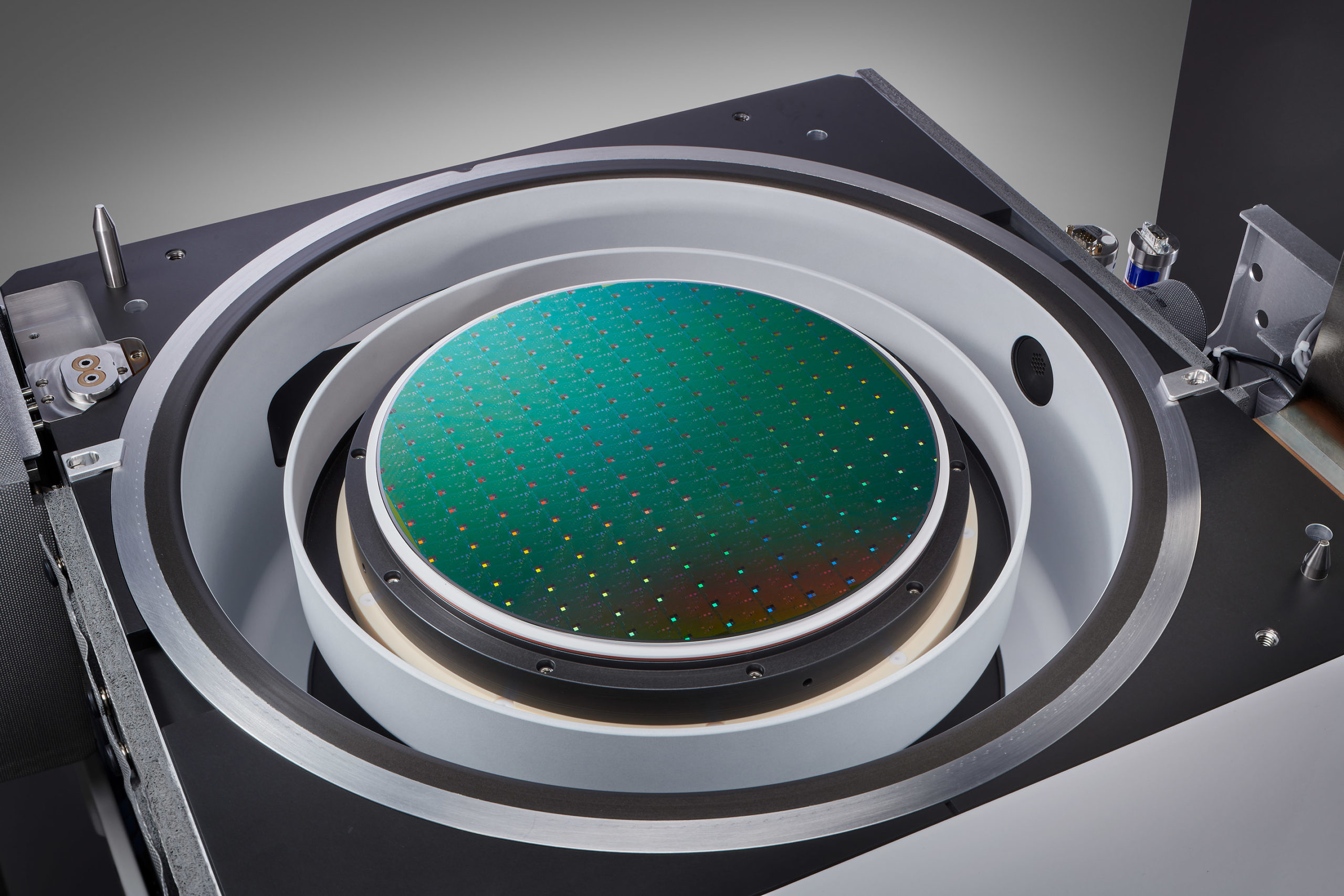
画期的なポートフォリオにより、3D アーキテクチャ、先端ロジックおよびファウンドリ用途向けに、0.1nm スケールの精度と超高選択性で等方的材料除去を実現します。
SEMulator3D
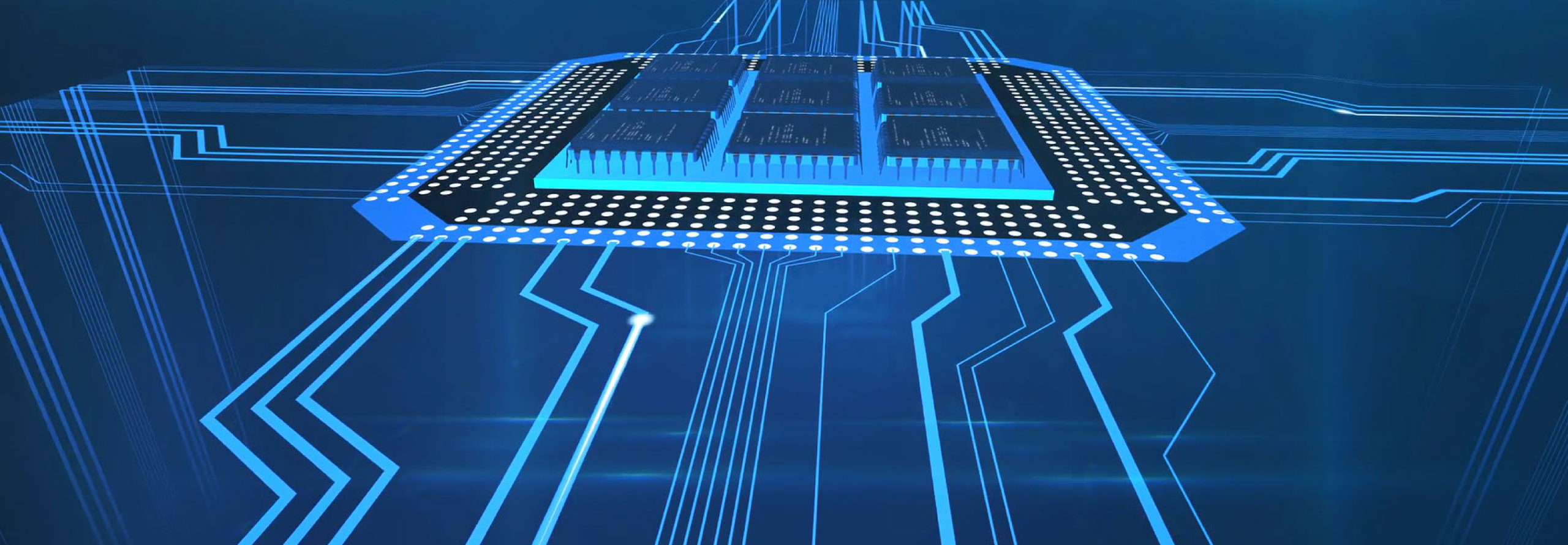
半導体プロセスモデリング・プラットフォーム SEMulator3D® は広範囲にわたる技術開発環境を提供します。
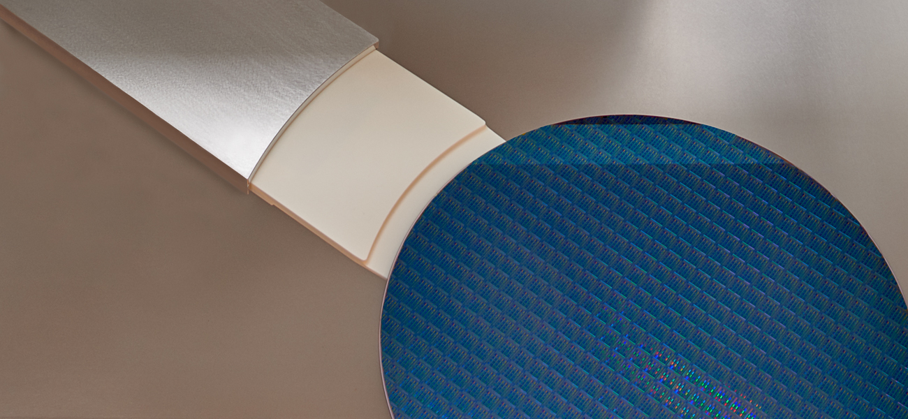
SENSE.I製品
私たちの最新エッチング装置のプラットフォームは、最高の生産性でプロセスパフォーマンスを提供するコンパクトで高密度のアーキテクチャで比類のないシステムインテリジェンスを実現します。
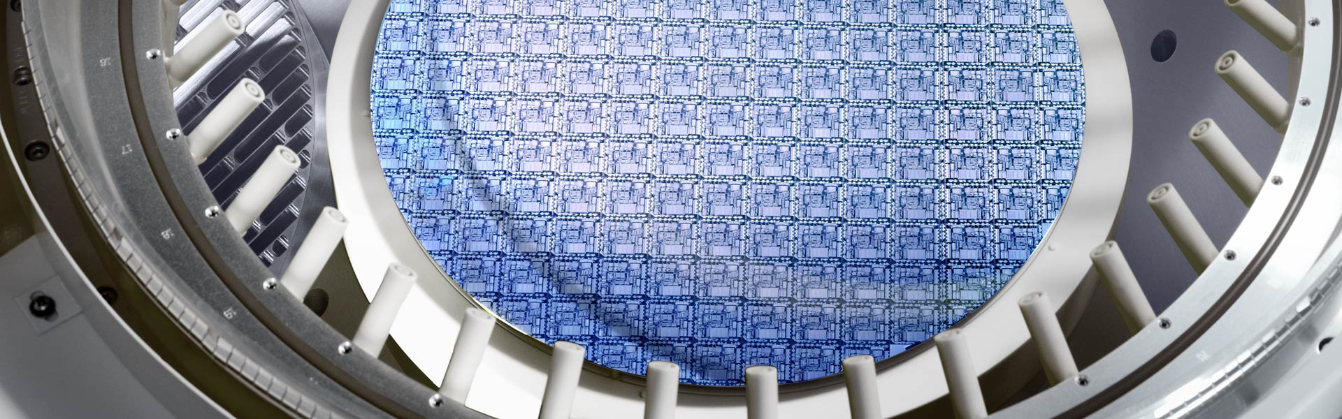
SPEED シリーズ製品
これらの酸化膜成膜製品は、業界最高のスループットと信頼性を備えた高アスペクト比スペースの完全なギャップフィル機能を提供します。
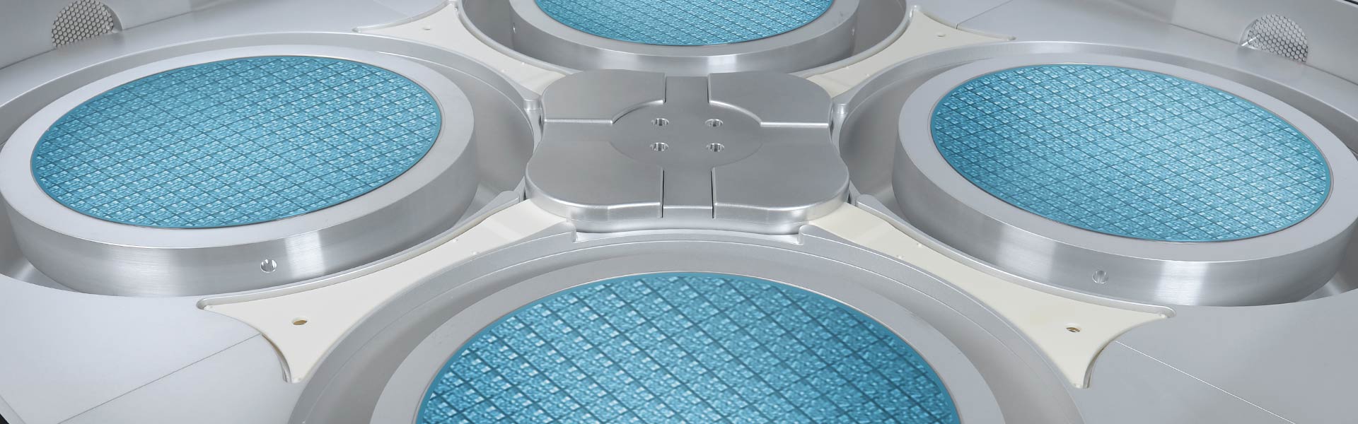
STRIKER シリーズ製品
高度なALD技術を活用することにより、これらの製品はナノスケールの機能を備えた高度なデバイスのクリティカルプロセスに対して優れた制御性能を実現する酸化膜を提供します。
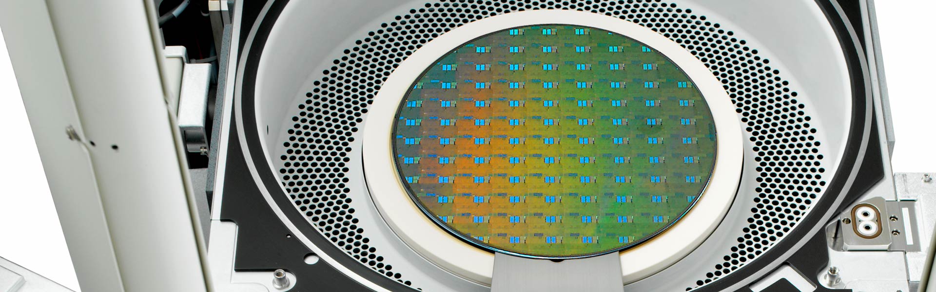
Syndion製品ファミリー
ディープエッチング用途では、高アスペクト比の重要な形状に必要な卓越したウェーハ全体にわたる均一性制御を提供します。
トリトン製品シリーズ
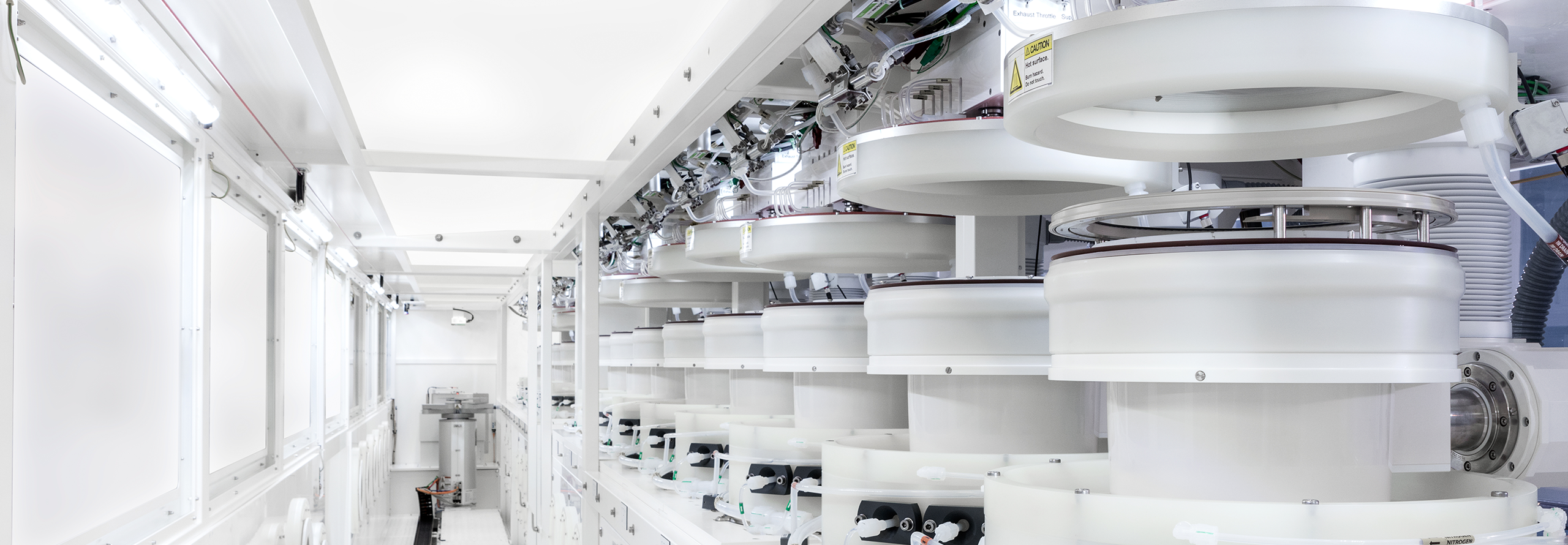
トリトンプラットフォームは、シングルウェハめっきおよびウェット処理用の汎用性の高いモジュール式ソリューションです。
VANTEX シリーズ製品
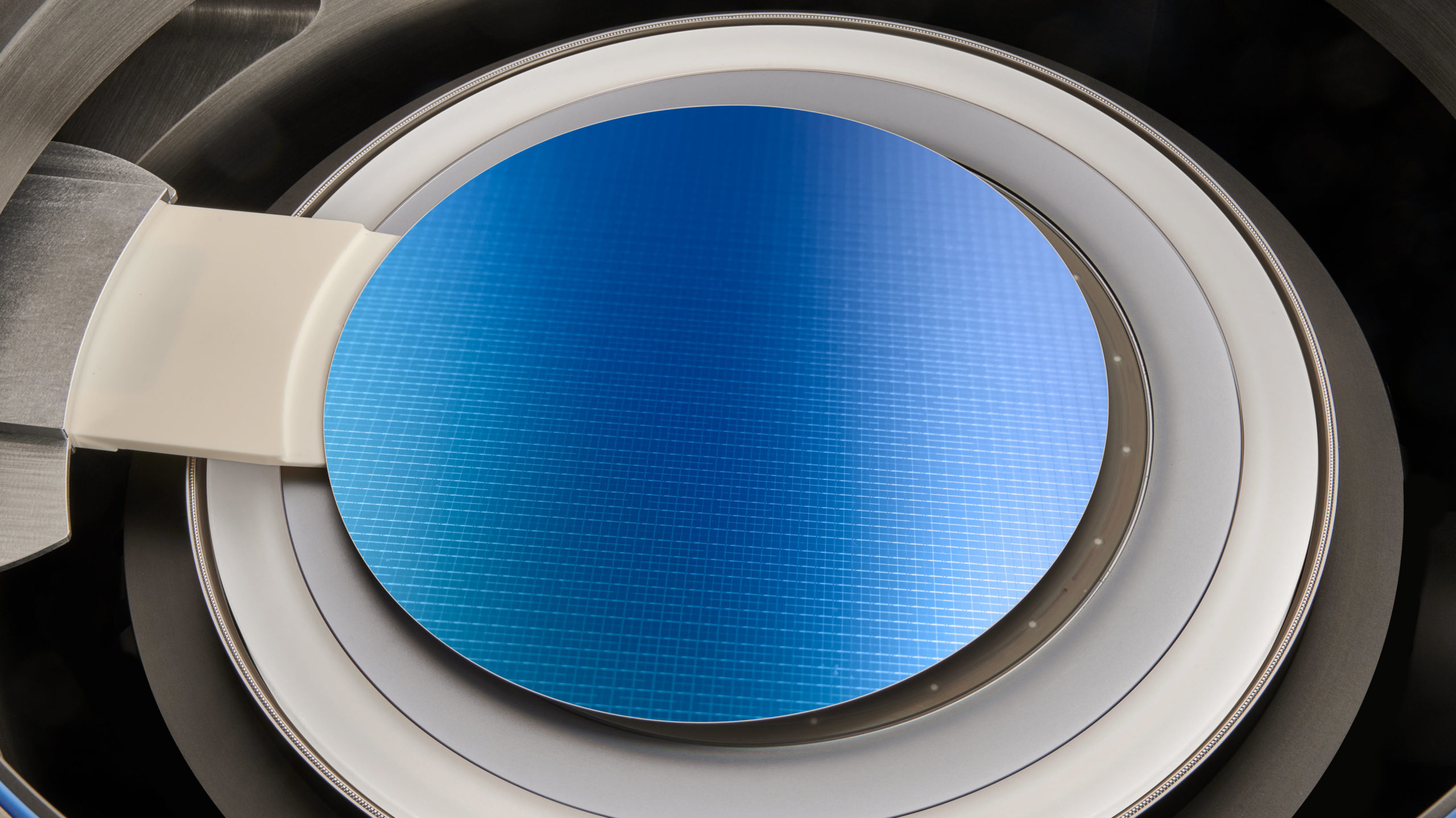
誘電体エッチングプロセスは、半導体デバイスの製造の中で非導電物質を除去します。特に業界最先端のメモリデバイスは、 ホールやトレンチの深さなどの難しい構造をもつため、厳しい公差で製造される必要があります。ラムリサーチの最新の誘電体エッチングシステムは、比類のない性能を実現し、厳しい高アスペクト比が求められるデバイスに生産性をもたらします。Vantex™は、進化したメモリデバイス製造の要件に対応する高度なRFテクノロジー、均一性制御およびEquipment Intelligence®を提供します。
VECTOR シリーズ製品
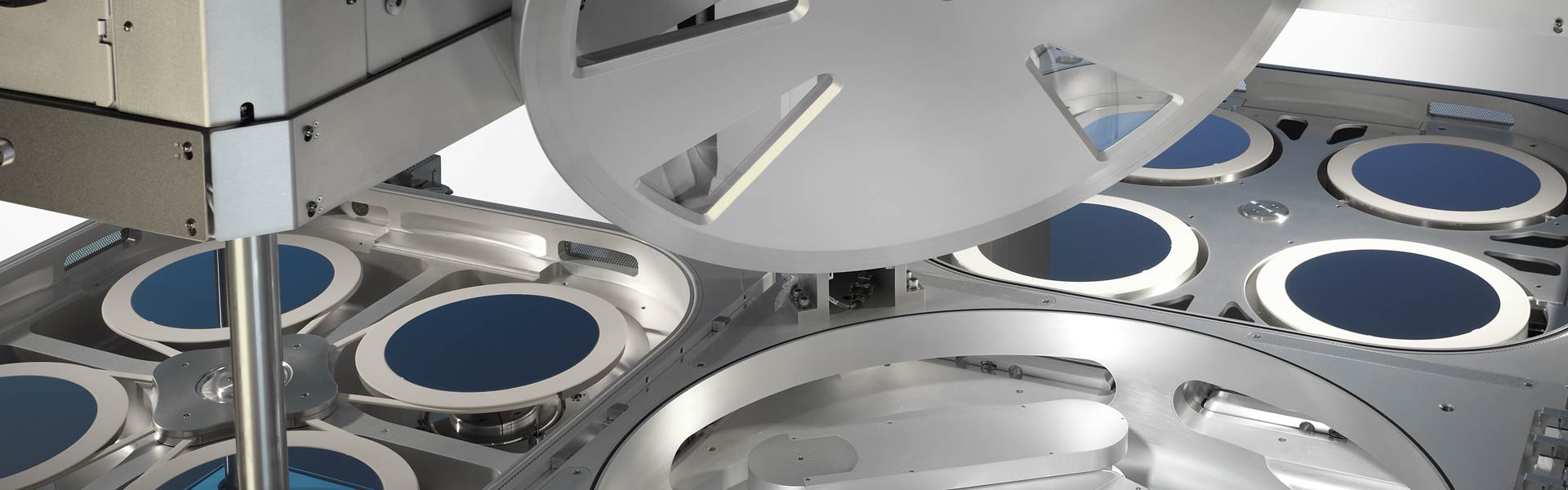
ラムリサーチ社のPECVD製品ファミリーは、幅広いデバイスアプリケーションに対応した高い生産性の精密な酸化膜成膜を提供します。
VERSYS METAL シリーズ製品
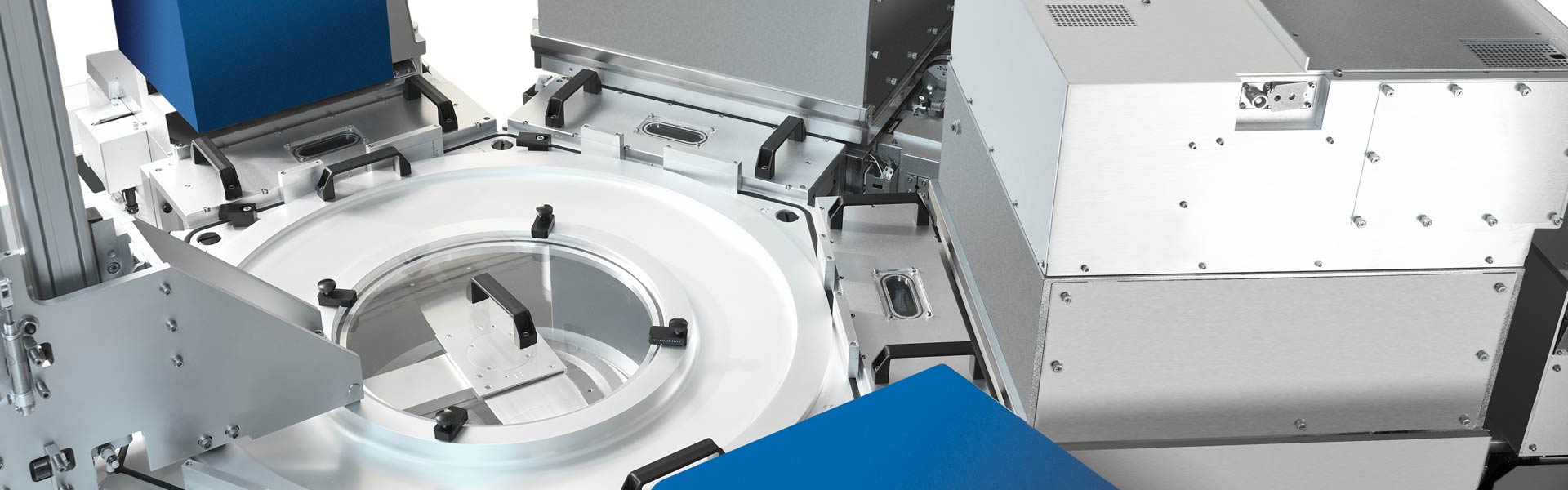
これらのメタルエッチング製品は、電気配線およびメタルハードマスク用途向けに高い生産性を備えたプロセス制御を提供します。
関連ブログ記事
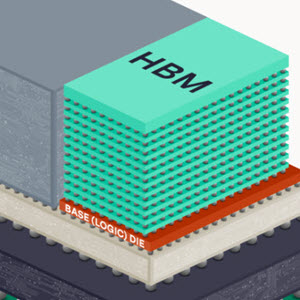
The Road to the AI Era Is Paved in Semiconductor Manufacturing Innovation
“The Road to the AI Era Is Paved in Semiconductor Manufacturing Innovation," an in-depth white paper written by The TechArena and sponsored by Lam Research, explores the pivotal role of chipmaking innovation in ushering in the next transformative technological age. The paper provides authoritative insights into the revolutionary effects of generative AI and large language models across various industries, the emerging challenges in delivering performance to meet these advanced requirements, and the critical importance of high bandwidth memory (HBM) in AI compute platforms.
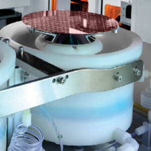
Will HBM Redefine What's Possible With AI?
There is a lot of buzz around high bandwidth memory (HBM). As artificial intelligence (AI) continues to advance so do its demands. Many major technology companies are betting on HBM to meet them. HBM is an advanced computer memory designed to offer faster data access with lower energy consumption. For AI, it can be a critical component in performance and reducing power consumption in memory chips.