从智能手机和平板电脑到计算机和游戏系统,电子设备的日益普及正在塑造技术的未来。 人工智能(AI)正在推动对更高效、更强大的工艺设备的需求。 半导体制造的主要进步集中在小型化、性价比和连接性上。
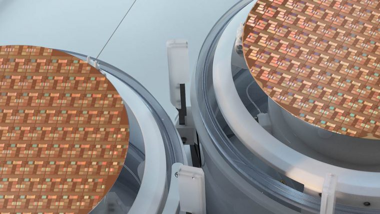
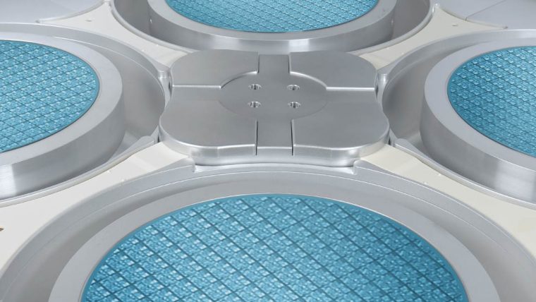
先进封装技术和chiplet设计对于满足下一代器件的需求至关重要。 晶圆级封装(WLP)、3D 硅通孔(TSV)互连和混合键合等技术越来越多地被应用,从而实现异构集成和系统级封装(SiP)解决方案。 在生成式AI的推动下,对计算能力永无止境的需求正在突破封装尺寸的界限,为大幅面面板级封装和先进的玻璃基板铺平了道路,使其成为高性能计算(HPC)的未来。 这些创新可实现将多个芯片集成到单个封装中,预示着器件性能和设计进入一个新时代。
封装
我们的解决方案WETS 产品线
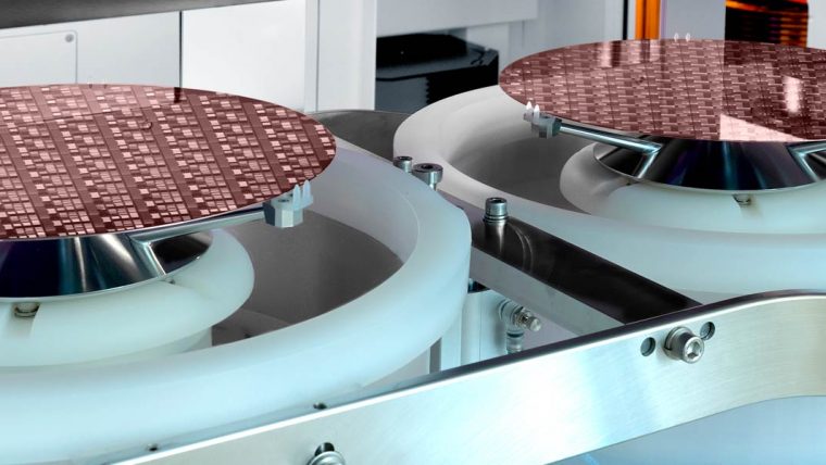
为电镀和湿法制程提供领先的解决方案,包括光刻胶剥离、刻蚀和清洗
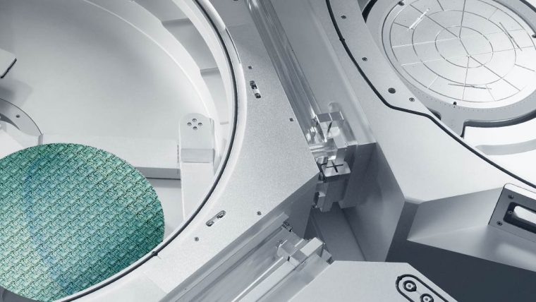
干法刻蚀解决方案
高生产力解决方案,以克服先进封装中的技术挑战,如高深宽比刻蚀(TSV、TDV和TGV)和等离子切割


介电和金属沉积
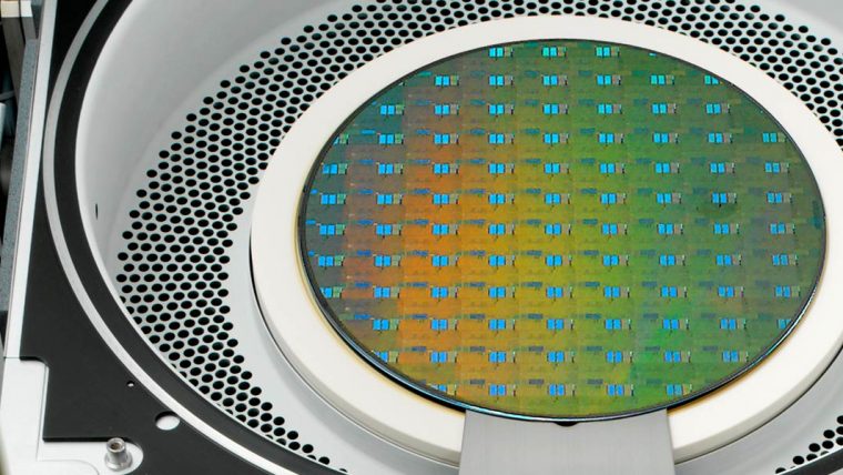
PECVD、ALD 和 CVD 金属的差异化解决方案。 实现先进封装的各种薄膜要求,包括高粘合强度介电、高质量的晶片间间隙填充薄膜、以及用于晶圆应力和形状管理的薄膜应力可调性

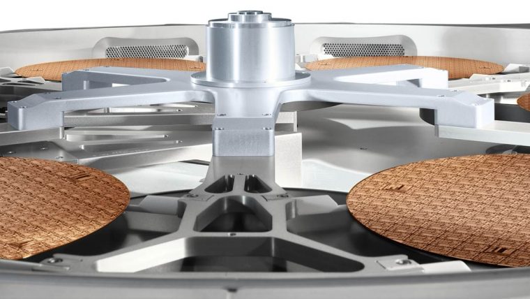
良率提高和过程控制
创新的解决方案,例如用于提高晶圆到晶圆键合良率的晶圆边缘管理,以及通过质量计量实现高生产量工艺控制能力,以克服新兴的先进封装应用的挑战


面板制程解决方案
将晶圆级工艺技术、性能和生产良率转移到面板级工艺。 为湿法面板制程提供差异化解决方案,例如铜重布线层、微凸块、TGV 和铜 堆积电镀、PR/PI 剥离/显影、刻蚀、粗化和清洗。