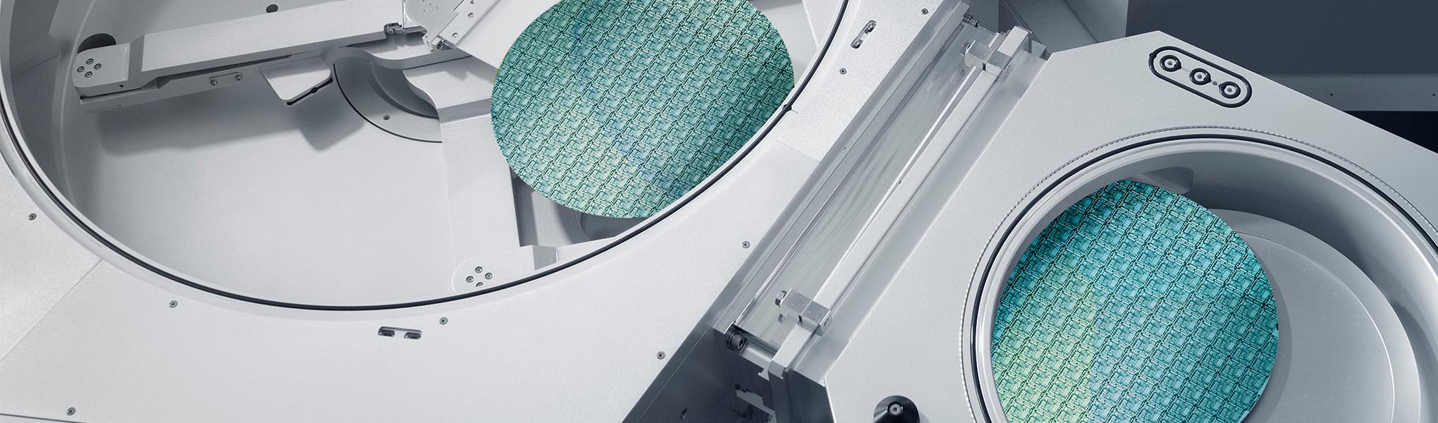
優れた薄膜を作る
成膜工程では、半導体デバイスの材料となる誘電膜(絶縁膜)と金属(導体)の薄膜層を形成します。使用する材料や配線槽の構造により成膜方法は異なります。電解メッキ(ElectroChemical Deposition:ECD)はIC内の素子を接続するCuの「電線(インターコネクト)」を作るのに使用します。Cuや他の金属メッキはシリコン貫通ビアやWLPの工程でも用いられます。微細なタングステンのプラグ形成には精密な化学気相成長(Chemical Vapor Deposition:CVD)や原子数個分の層を少しずつ堆積する原子層成膜(Atomic Layer Deposition:ALD)を使います。プラズマCVD(PECVD)、高密度プラズマCVD(HDP-CVD)およびALDは電気素子を保護・絶縁するのに極めて大事な役割を果たす絶縁膜を形成するのに利用されます。
材料の種類とパターン形状が複雑になり、デバイス製造のハードルがますます高くなるなか、ラムリサーチの成膜製品は、必要な精度、性能、柔軟性を提供します。
ラムリサーチの製品
成膜
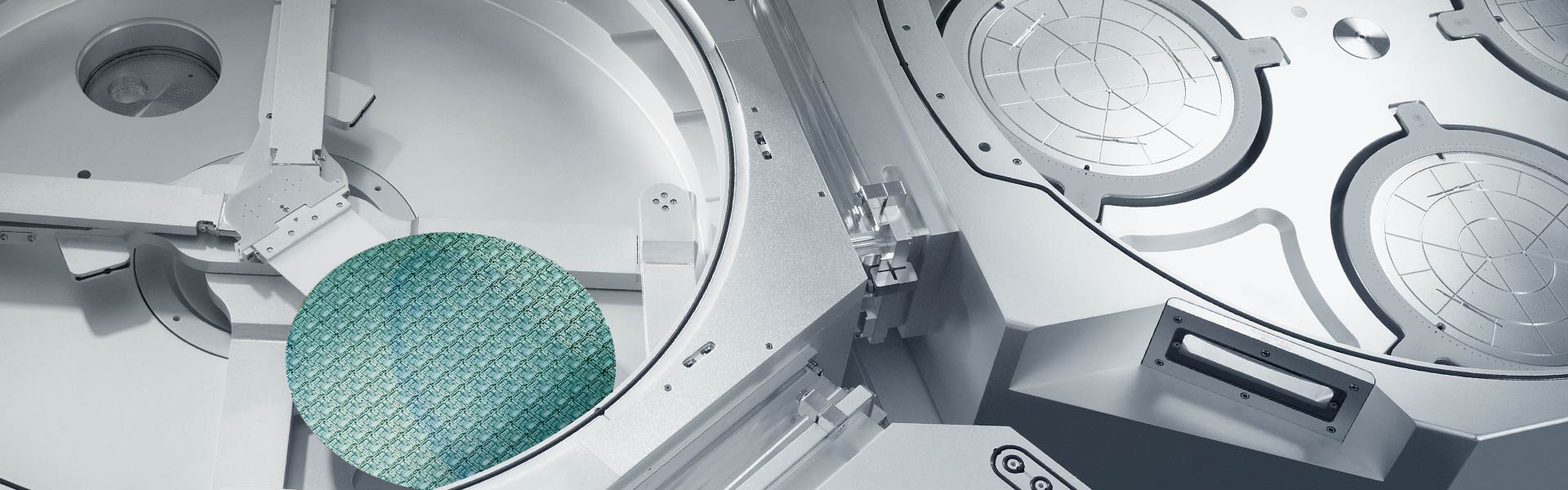
ALTUS製品ファミリー
CVDとALD技術を組み合わせた市場をリードするこれらのシステムにより、先進的なタングステンメタライゼーション用途向けに高コンフォーマルな金属膜を成膜します。

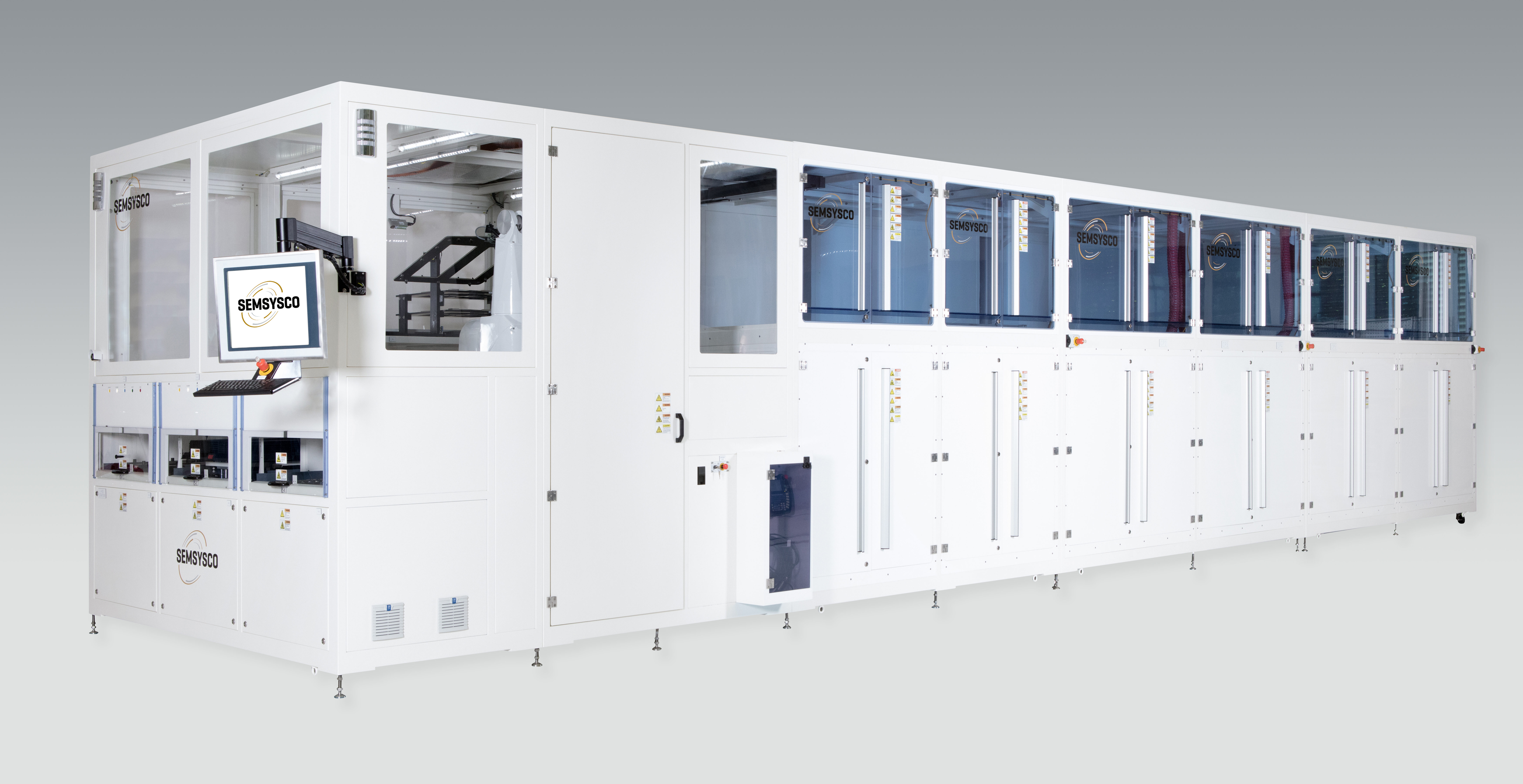
カリスト製品シリーズ
半導体業界のニーズに合わせた、300×300mmからGen5.1(1100x1300mm)までの基材をウェット処理するための先進的な縦型加工プラットフォーム。
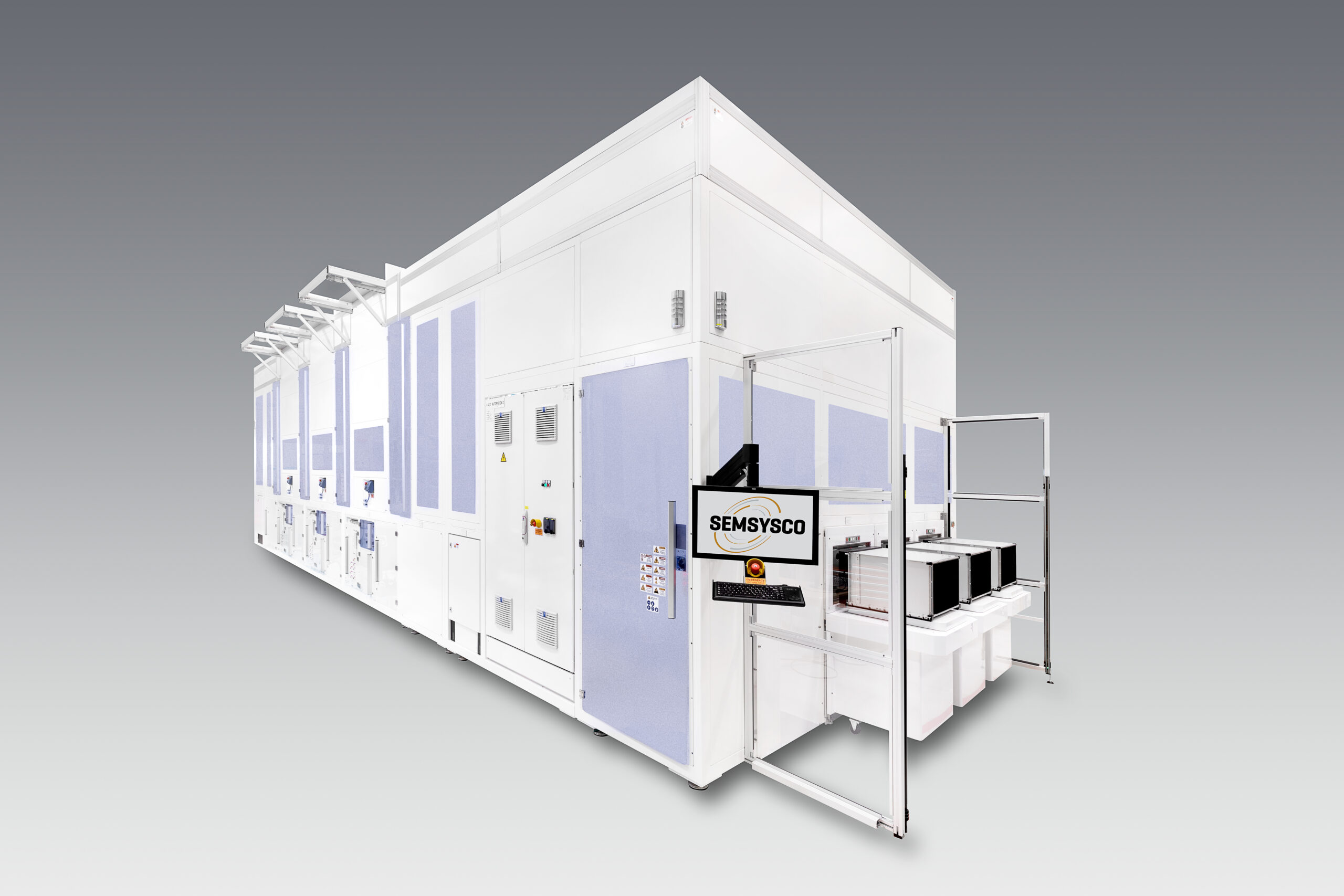
フェニックス製品シリーズ
フェニックスは510x515mm 基板用の全自動大量パネル加工を提供します。
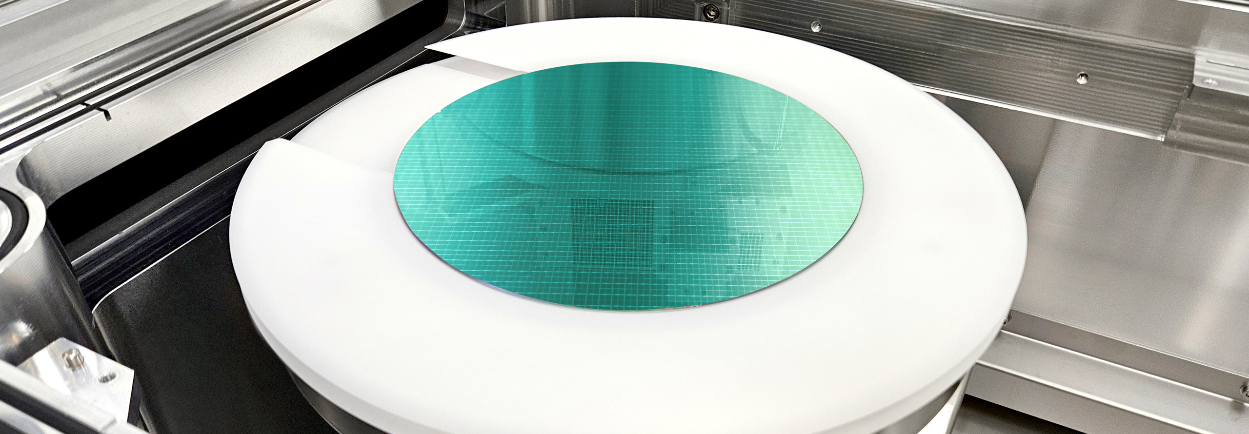
Prestis™
弊社のPrestis™製品は、スペシャルティテクノロジー向けに、幅広い複雑な多元材料の薄膜成膜ソリューションを提供します。
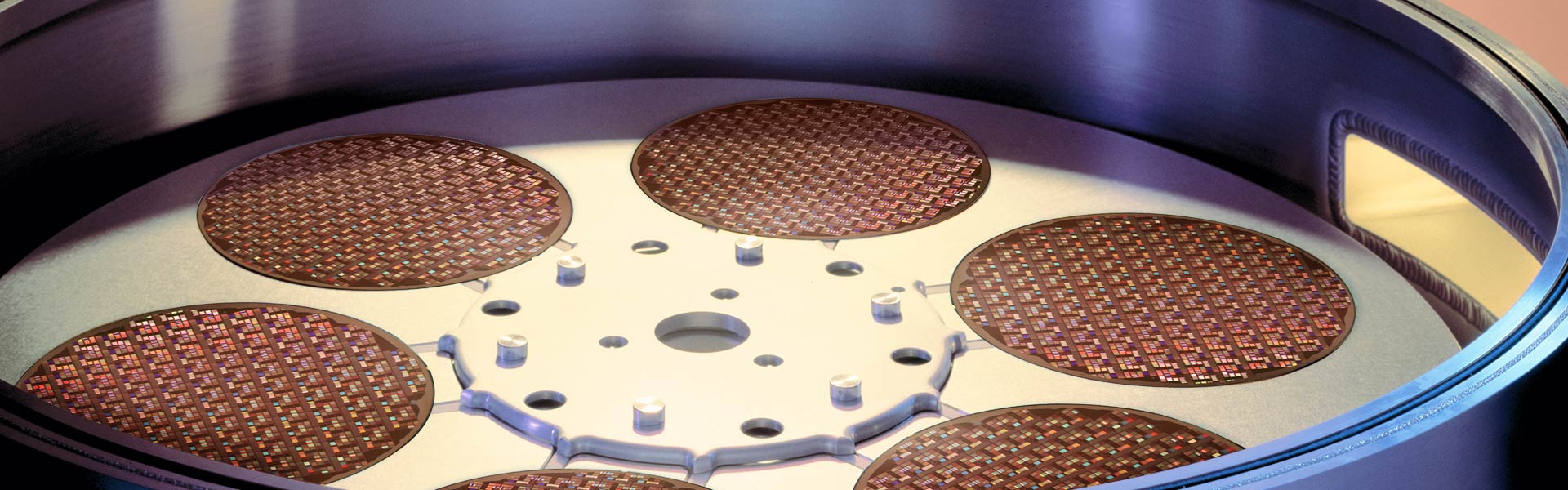
RELIANT成膜製品
RELIANT 成膜製品は、スペシャルティ・テクノロジーのロードマップを実現し、ファブの生産寿命を延ばします。
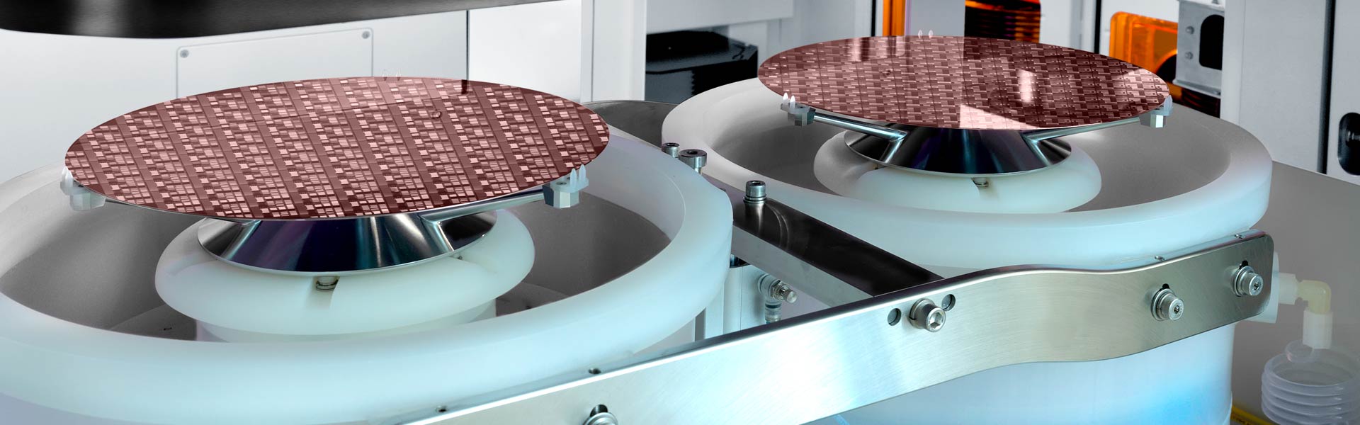
SABRE 3D シリーズ製品
一品および再生されたReliant製品は、コンダクター膜、酸化膜、および金属エッチング アプリケーションにおいて低所有コスト(低いランニングコスト)で、高信頼性、実証済みのソリューションを提供します。
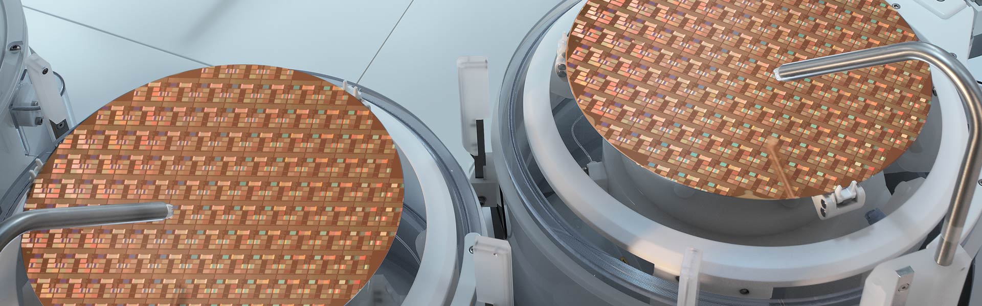
SABRE シリーズ製品
実績のあるElectrofill技術により、これらの高生産性システムは高度なパッケージングアプリケーションを開発するための高品質な金属膜を提供します。
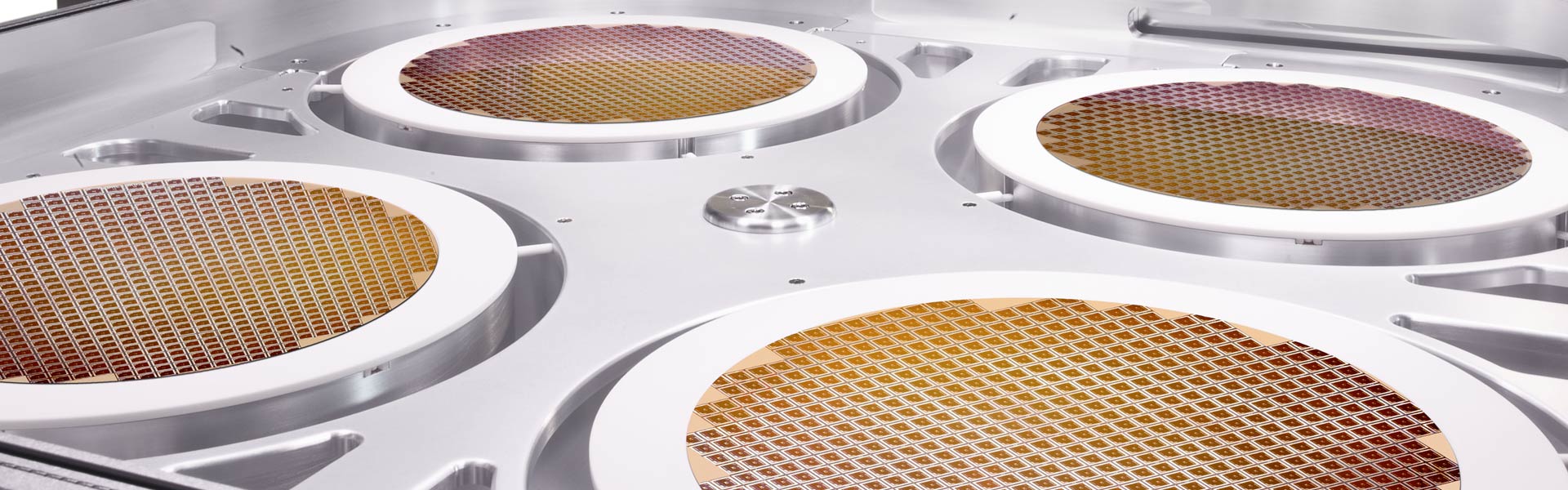
SOLA シリーズ製品
このシリーズ製品は、高度な膜アプリケーションの物理的特性を向上させる特殊な成膜後のトリートメント機能を提供します。
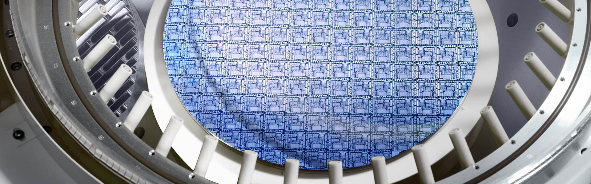
SPEED シリーズ製品
これらの酸化膜成膜製品は、業界最高のスループットと信頼性を備えた高アスペクト比スペースの完全なギャップフィル機能を提供します。
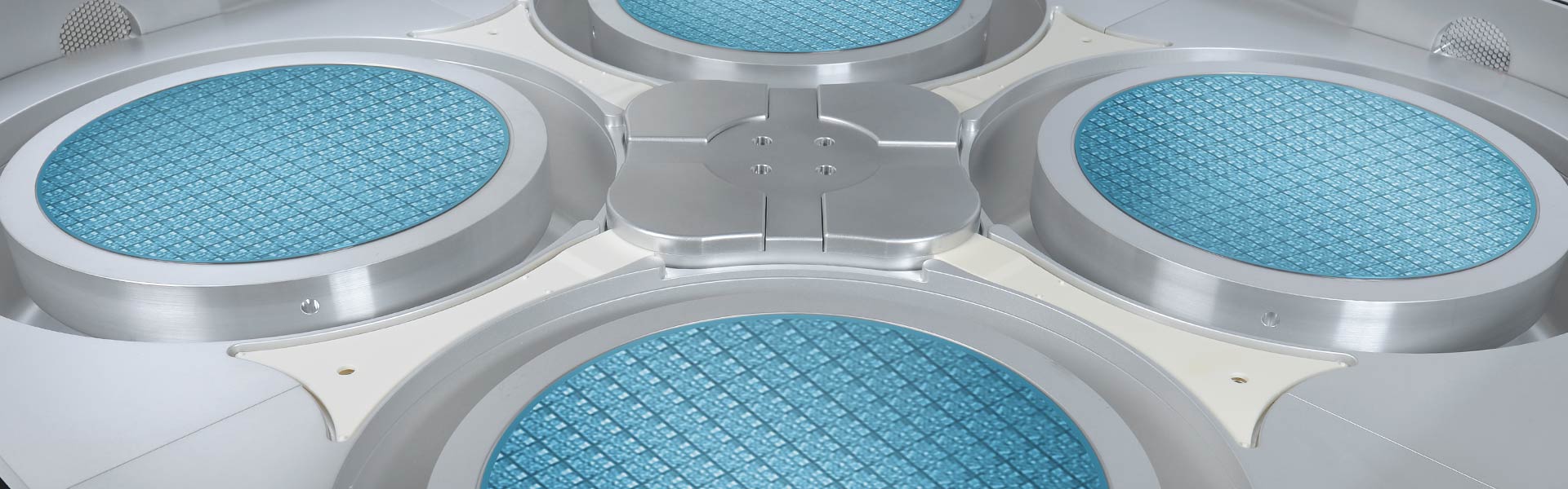
STRIKER シリーズ製品
高度なALD技術を活用することにより、これらの製品はナノスケールの機能を備えた高度なデバイスのクリティカルプロセスに対して優れた制御性能を実現する酸化膜を提供します。
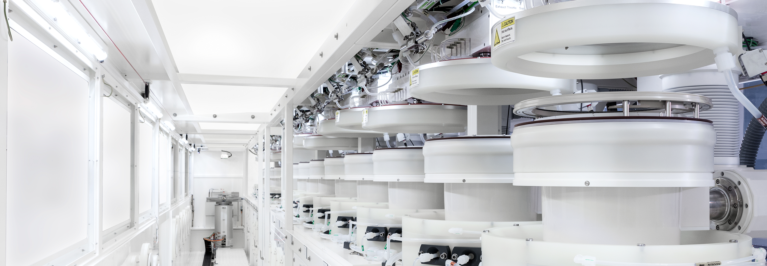
トリトン製品シリーズ
トリトンプラットフォームは、シングルウェハめっきおよびウェット処理用の汎用性の高いモジュール式ソリューションです。
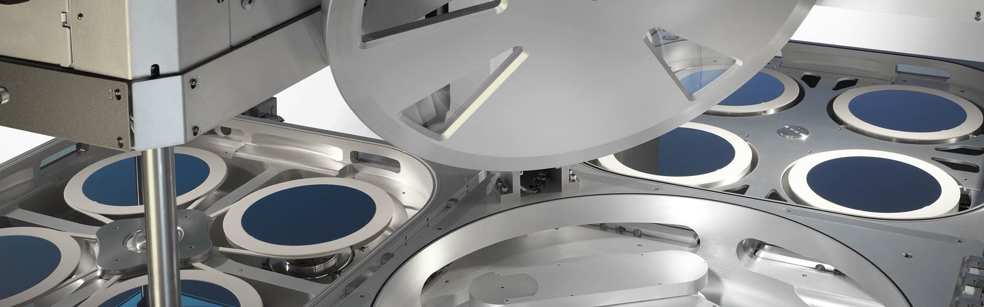
VECTOR シリーズ製品
ラムリサーチ社のPECVD製品ファミリーは、幅広いデバイスアプリケーションに対応した高い生産性の精密な酸化膜成膜を提供します。
関連ブログ記事
Lam’s Laser Focus on the Future of Chip Manufacturing
Lam Research hopes to revolutionize microchip manufacturing with the launch of a new system: Prestis™. Why it matters: For the first time in semiconductor production, Lam is using lasers to deposit thin films and bringing pulsed laser deposition (PLD) to wafer-level mass production. Prestis is expected to be key in developing cutting-edge specialty technologies devices, such as RF (radio frequency) filters for 5G and Wi-Fi 6 and high-end MEMS (micro-electromechanical systems) microphones.
Introducing Coronus DX, World’s First Bevel Deposition Solution Optimized for 3D Chipmaking
For more than 15 years, Lam’s Coronus® product family has been the leader in wafer bevel technology. Today we introduced the newest member of the family, Coronus DX. It’s the industry’s first bevel deposition solution optimized to tackle key manufacturing challenges in next-gen logic, 3D NAND and advanced packaging applications.