
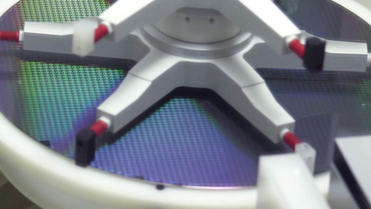
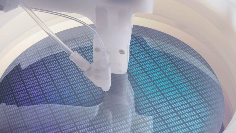
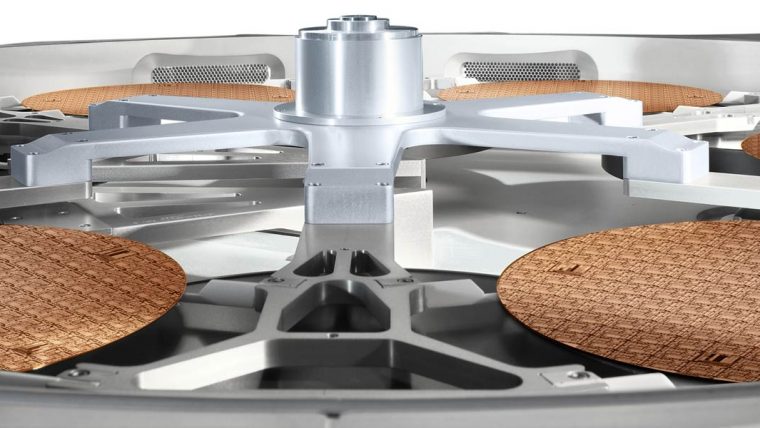
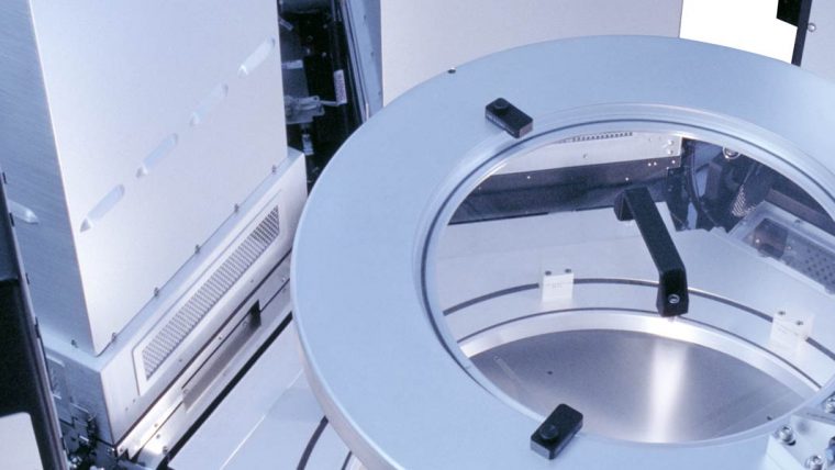
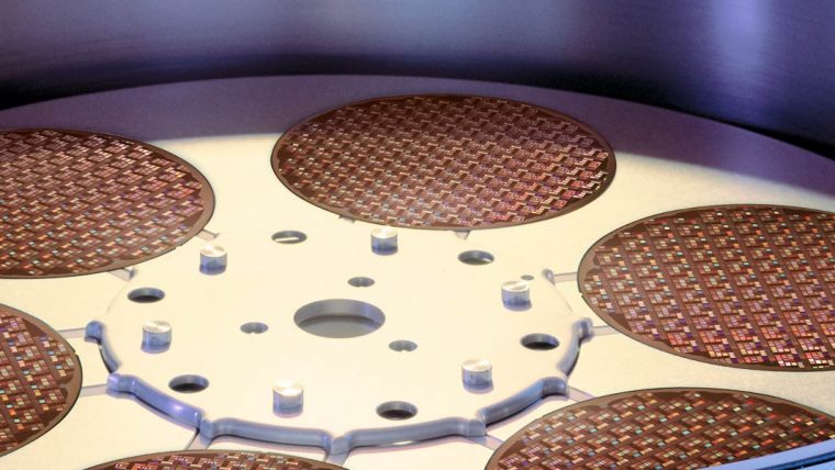
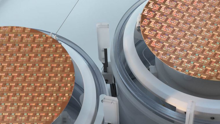
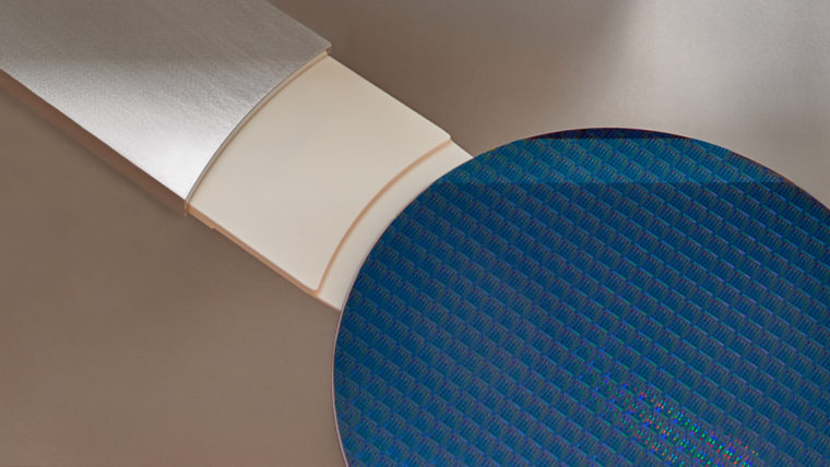
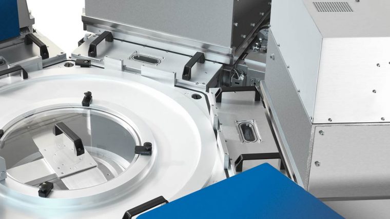
互连由复杂的布线构成,连接着芯片上数十亿个组件(晶体管、电容等)。随着器件不断变小、封装密度不断加大,需要更多的互连层次,而要把一切都连接起来,挑战性必然越来越大。事实上,随着构件尺寸继续缩小,互连已成为当今最先进的芯片的速度瓶颈。因此,我们需要能尽量降低金属互连电阻的技术以及能提升隔离能力的新型介电材料。为了生产最新的高性能电子器件,先进互连结构具有尺寸狭小、薄膜层复杂的特点,这需要越来越灵活和精密的加工能力。
互连
我们的解决方案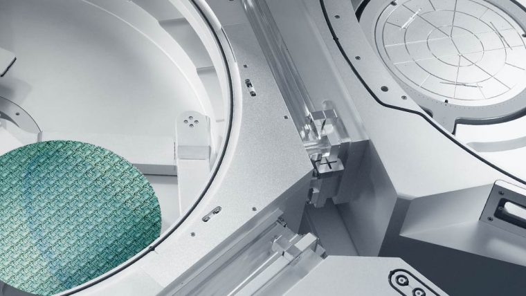


Fabtex™ Yield Optimizer
Semiconductor Yield Optimization Platform
Fabtex™ Yield Optimizer is a cutting-edge software platform designed to help semiconductor foundries accelerate yield ramp and improve high-volume manufacturing performance.


Related Blog Posts
-
Will Moly Replace Tungsten in Semiconductors?
Feb 1, 2024To keep pace with Moore's Law and enable greater interconnect scaling, the semiconductor ecosystem is continually experimenting with variations of materials. Tungsten has been the interconnect metal of choice for nearly a quarter century in NAND, DRAM, and logic/foundry middle-of-line applications. But scaling requirements are now pushing the boundaries of what is possible with tungsten. A variety of metals are being considered, but one — molybdenum — is an especially promising candidate. At the atomic dimensions required for advanced chipmaking, moly is emerging as the most suitable material to replace tungsten, creating a major inflection in the industry.
-
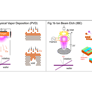
A Deposition and Etch Technique to Lower Resistance of Semiconductor Metal Lines
Mar 22, 2023Cu’s resistivity depends on its crystal structure, void volume, grain boundaries and material interface mismatch, which becomes more significant at smaller scales. The formation of Cu wires is traditionally done by etching a trench pattern in low-k silicon dioxide using a trench etch process, and subsequently filling the trench with Cu via a damascene flow. Unfortunately, this method produces multi-crystalline structures with significant grain boundaries and voids, which increases the Cu wire resistance. A highly resistive TaN liner material is also utilized in this process to prevent Cu diffusion during the damascene annealing process.