The future of technology is being shaped by the increasing prevalence of electronic devices, from smartphones and tablets to computers and gaming systems. The push for artificial intelligence (AI) is driving the need for more efficient and powerful processing hardware and demanding new semiconductor architectures.
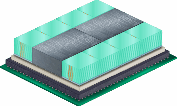
Advanced packaging is a key enabler for overcoming traditional scaling limits and meeting future computing needs. In addition to shrinking transistors, chipmakers are looking beyond the chip into diverse packaging architectures that enhance processing power, memory, speed, and energy efficiency through 3D integration and chiplet technologies.
A pivotal moment for
advanced packaging
Advanced packaging technologies and chiplet designs are essential for meeting the demands of next-generation devices in our technological future. Without solving for today’s advanced packaging challenges, the AI revolution will stall just as it begins to transform the industry.
Without continued advancement in advanced packaging technologies, industries counting on AI-driven transformation—from healthcare to transportation to energy—will see their innovation roadmaps extended by years, not quarters.
This pivotal moment will determine how quickly humanity can solve its most pressing problems through computational advances. The ability to overcome today’s advanced packaging hurdles will directly impact our capacity to develop life-saving medical treatments, create sustainable energy solutions, and build intelligent systems that will define our future prosperity.
How Lam Research is driving innovation forward
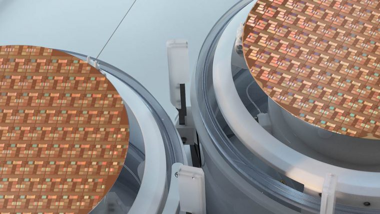
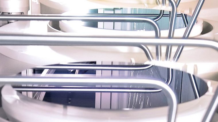
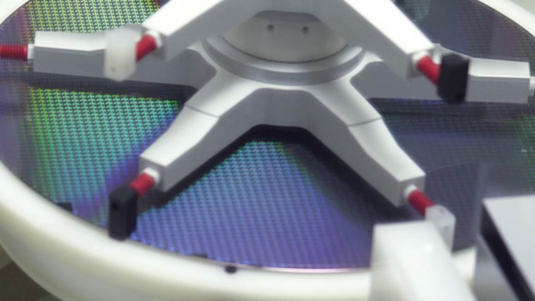
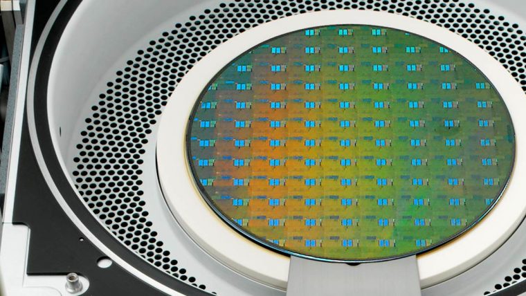
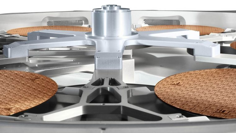
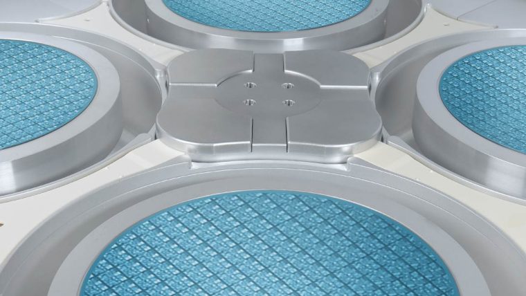
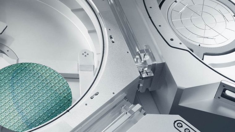
From plating to etch, advanced packaging requires extreme precision at each step of the chipmaking process. Lam’s approach leverages our decades of leadership in etch and deposition to deliver best-in-class products that address our customers’ toughest challenges with unmatched precision and performance.
Lam’s advanced packaging portfolio centers on three critical innovation areas that address the semiconductor industry’s most pressing challenges:
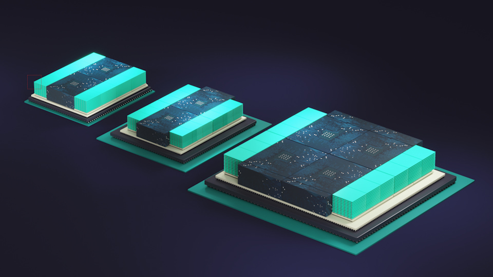
- Large-Format Package Interconnect Leadership: Enabling larger AI packages—scaling from 3.3x to 5.5x to 9x reticle size—across both wafer and panel platforms to meet the growing demands of high-performance computing.
- High-Yield Die-to-Wafer (D2W) Assembly: Driving innovations in materials and process solutions for increasingly critical applications in die-to-wafer bonding that enable advanced memory and logic scaling.
- Novel Wafer Shape/Stress Management: Pioneering solutions for 3D wafer-on-wafer (3D-WoW) stacking that address critical challenges in wafer bowing, twisting, and bond integrity.
Our Solutions
Lam’s advanced packaging portfolio enables more powerful AI accelerators to
- Overcome the memory wall
- Support increased I/O count
- Allow for more energy-efficient computing
—all while maintaining reliability and yield essential for commercial success.
Our advanced packaging solutions deliver superior technical performance across all critical parameters: uniformity, yield, process control, and throughput. With industry-leading metrology integration and process capabilities, Lam tools provide the precision and reliability required for today’s most challenging packaging applications.
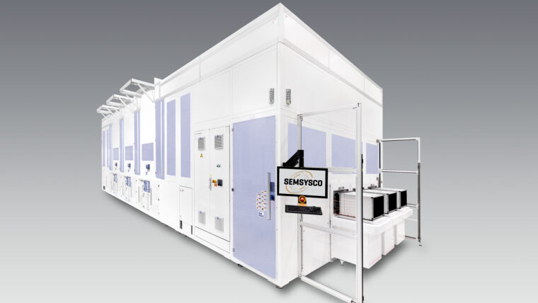
WETS Product Line
Delivering leading solutions in electroplating and wet processing including photoresist strip, etch and clean
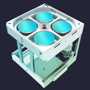
SABRE 3D Product Family
Electrochemical Deposition (ECD)
Using our proven Electrofill technology, these high-productivity systems deliver quality metal films for advanced packaging applications.
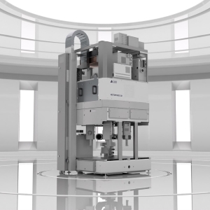
SABRE Product Family
Electrochemical Deposition (ECD)
This product family offers precision metal plating for copper damascene manufacturing on the industry’s productivity-leading ECD platform.
SP Series Product Family
Wet Clean
This proven product family delivers reliable, cost-efficient wet clean/wet etch solutions that gently remove unwanted materials from the wafer.
DV-Prime & Da Vinci Product Families
Wet Clean
These products provide the process flexibility needed with high productivity to address multiple wafer cleaning steps throughout manufacturing.
Dry Etch Solutions
High-productivity solutions to overcome technically challenging requirements in advanced packaging, such as high-aspect -ratio etch (TSV, TDV & TGV) and plasma dicing
Syndion Product Family
Deep Reactive Ion Etch (DRIE) Reactive Ion Etch (RIE)
For deep etch applications, this product family provides the exceptional across-wafer uniformity control needed for critical high aspect ratio features.

Flex Product Family
Atomic Layer Etch (ALE) Cryogenic Etching Reactive Ion Etch (RIE)
Our dielectric etch systems offer application-focused capabilities for creating a wide range of challenging structures in advanced devices.

Kiyo Product Family
Reactive Ion Etch (RIE)
These market-leading conductor etch products deliver the high-performance precision and control at high productivity needed for critical device features.
GAMMA Product Family
Dry Strip
These products provide the process flexibility needed to address a wide range of critical photoresist strip applications.
Dielectric and Metal Deposition
Differentiated solutions for PECVD, ALD, and CVD metals. Enabling various film requirements for advanced packaging, including high-bond- strength dielectric, high quality inter-die gapfill film, and film stress tunability for wafer stress and shape management

VECTOR Product Family
Plasma-Enhanced Chemical Vapor Deposition (PECVD)
Our PECVD product family provides precise dielectric film deposition at high productivity for a wide range of device applications.
Striker Product Family
Atomic Layer Deposition (ALD)
Using advanced ALD technology, these products deliver dielectric films with exceptional control for critical processes in advanced devices with nanoscale features.
ALTUS Product Family
Atomic Layer Deposition (ALD) Chemical Vapor Deposition (CVD)
Combining CVD and ALD technologies, these market-leading systems deposit highly conformal metal films for advanced tungsten metallization applications.
Yield Improvement and Process Control
Innovative solutions to overcome challenges of emerging advanced packaging applications, such as wafer bevel management for wafer-to-wafer bonding yield improvement and high- throughput process control capability with mass metrology

Coronus Product Family
Plasma Bevel Etch and Deposition
Coronus systems focus on the bevel edge to enhance overall yield. Semiconductor processing can cause residues and roughness to accumulate along the wafer edge where they may flake off, drift to other areas, and create defects that cause a device to fail. Coronus etch products remove bevel residues and Coronus deposition protect the wafer bevel from damage.

Metior Product Family
Mass Metrology
Our mass metrology systems deliver sub-milligram measurement capability for advanced process monitoring and control of three-dimensional device structures.
Panel Processing Solutions
Transferring wafer-level processing technology, performance, and production yield, to panel-level processing. Delivering differentiated solutions for wet panel processing, such as Cu RDL, micro-bump, TGV and Cu build-up electroplating, PR/PI strip/develop, etch, roughening, and clean.
Kallisto Product Family
Electrochemical Deposition (ECD)
An advanced vertical processing platform for wet chemical treatment of substrates from 300x300mm up to Gen 5.1 (1100 x 1300mm) tailored to the needs of semi industry.
Phoenix Product Family
Electrochemical Deposition (ECD) PR-Development PR-Strip Wet Clean/Strip
Phoenix offers a fully-automated high volume panel processing for 510x515mm substrates.
Additional Resources
-
Lam Research Introduces VECTOR TEOS 3D to Address Critical Advanced Packaging Challenges in Chipmaking
September 9, 2025 -
Everything You Need to Know About VECTOR TEOS 3D
September 9, 2025