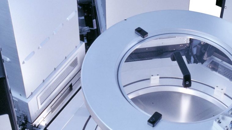
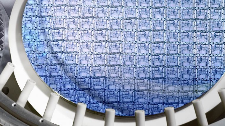
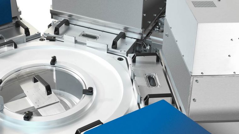
Discrete devices are single semiconductors like diodes or transistors. Power transistors are an important class of discrete devices and are used in a range of applications to regulate voltages, help lower power consumption, and reduce heat generation. For example, they are essential components in circuits aimed at extending battery life in portable electronics. Emerging wide-bandgap power devices (e.g., GaN and SiC) offer both low- and high-power applications at higher frequencies, addressing consumer electronics as well as higher-power applications in the power grid, energy, transportation, and automotive sectors. Examples of key power devices based upon silicon or wide-bandgap materials include power diodes, thyristors, power metal-oxide semiconductor field effect transistors (MOSFETs), and insulated gate bipolar transistors (IGBTs). These specialty devices require low-cost manufacturing from reliable, high-productivity, and cost-effective equipment.
Discretes & Power Devices
Our SolutionsDSiE Product Family
Deep Reactive Ion Etch (DRIE)
These products deliver exceptional process control at high productivity for several critical and non-critical deep silicon etch applications.
DV-Prime & Da Vinci Product Families
Wet Clean
These products provide the process flexibility needed with high productivity to address multiple wafer cleaning steps throughout manufacturing.
Flex Product Family
Atomic Layer Etch (ALE) Cryogenic Etching Reactive Ion Etch (RIE)
Our dielectric etch systems offer application-focused capabilities for creating a wide range of challenging structures in advanced devices.
Kallisto Product Family
Electrochemical Deposition (ECD)
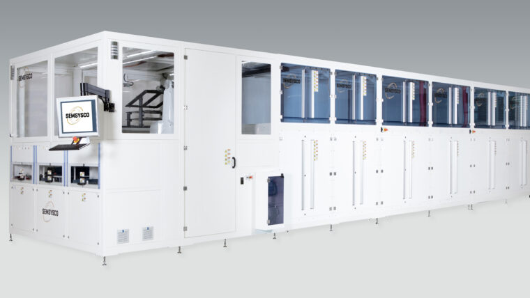
An advanced vertical processing platform for wet chemical treatment of substrates from 300x300mm up to Gen 5.1 (1100 x 1300mm) tailored to the needs of semi industry.
Kiyo Product Family
Reactive Ion Etch (RIE)
These market-leading conductor etch products deliver the high-performance precision and control at high productivity needed for critical device features.
Metior Product Family
Mass Metrology
Our mass metrology systems deliver sub-milligram measurement capability for advanced process monitoring and control of three-dimensional device structures.
OverViz
Plasma Modeling
OverViz™ is an industrial simulation software platform for high-fidelity modeling of plasma discharges.
Phoenix Product Family
Electrochemical Deposition (ECD) PR-Development PR-Strip Wet Clean/Strip
Phoenix offers a fully-automated high volume panel processing for 510x515mm substrates.
Reliant Clean Products
Reliant Systems Wet Clean/Strip
Our Reliant clean products enable roadmaps for Specialty Technologies and extend the productive life of fabs.
Reliant Deposition Products
Chemical Vapor Deposition (CVD) High-Density Plasma Chemical Vapor Deposition (HDP-CVD) Plasma-Enhanced Chemical Vapor Deposition (PECVD) Pulsed Laser Deposition (PLD) Reliant Systems
Our Reliant deposition products enable roadmaps for Specialty Technologies and extend the productive life of fabs.
Reliant Etch Products
Deep Reactive Ion Etch (DRIE) Reactive Ion Etch (RIE) Reliant Systems
Our Reliant etch products enable roadmaps for Specialty Technologies and extend the productive life of fabs.
SP Series Product Family
Wet Clean
This proven product family delivers reliable, cost-efficient wet clean/wet etch solutions that gently remove unwanted materials from the wafer.
SPEED Product Family
High-Density Plasma Chemical Vapor Deposition (HDP-CVD)
These dielectric deposition products provide complete gapfill of high aspect ratio spaces with industry-leading throughput and reliability.
Triton Product Family
Electrochemical Deposition (ECD) Wet Clean/Strip
The Triton platform is a versatile and modular solution for single wafer plating and wet processing.
VECTOR Product Family
Plasma-Enhanced Chemical Vapor Deposition (PECVD)
Our PECVD product family provides precise dielectric film deposition at high productivity for a wide range of device applications.
Versys Metal Product Family
Reactive Ion Etch (RIE)
These metal etch products provide excellent process control at high-productivity for electrical connection and metal hardmask applications.
Recent Blog Posts
-

Advanced Packaging Furthers 3D Semi Structures and Extends Moore’s Law
May 20, 2024New developments in semiconductor packaging are contributing to the quest to extend Moore’s Law, the predictive model of adding more transistors to a semiconductor. One promising development is advanced packaging, which can better manage the power consumption of a collection of chips while shrinking their total size.
-
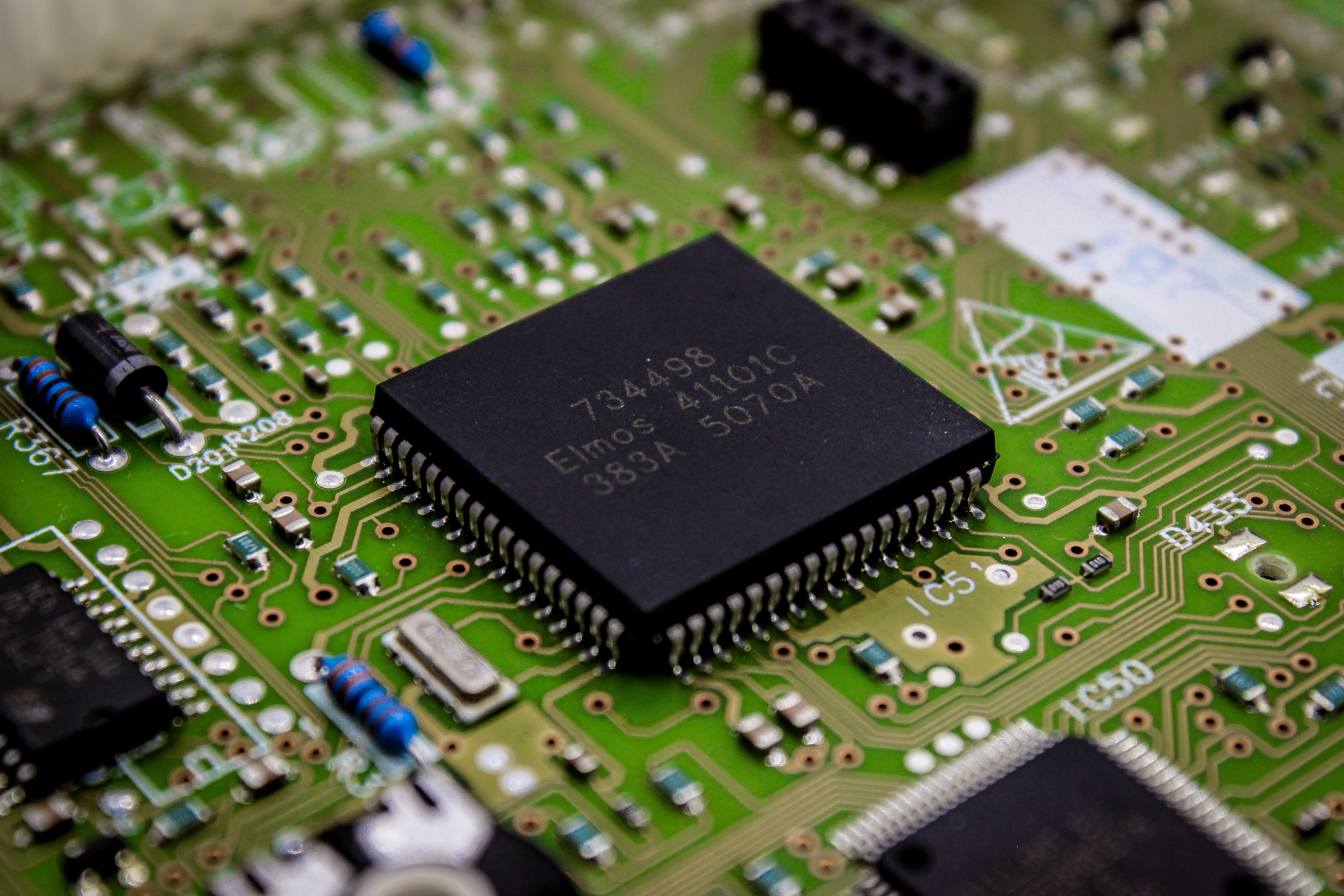
Heterogeneous Integration Sets Up an Inflection in Panel Processing Equipment (Drivers)
Mar 17, 2023The accelerating costs of transistor scaling are pushing the industry to find innovative ways to improve chip and system performance from generation to generation. That’s why heterogenous integration (HI) has become the latest inflection in packaging technology.
